- PCB Etching Machine: From Dragon Etching
- Purpose: PCB etching machines are used to selectively remove unwanted copper from the surface of a copper-clad board to create the desired circuit pattern.
- Process:
- The PCB is first cleaned to remove any contaminants.
- A layer of photoresist is applied to the board’s surface.
- A photomask, containing the desired circuit pattern, is aligned and placed on the board.
- The board is exposed to UV light, which hardens the photoresist in areas not covered by the mask.
- The etching machine sprays an etchant (e.g., ferric chloride) onto the board, which dissolves the exposed copper, leaving behind the circuit traces.
- After etching, the remaining photoresist is stripped to reveal the clean copper traces.
- Key Components: The machine includes a conveyor system for transporting boards, nozzles for uniform etchant distribution, and chemical control systems to monitor and control the etching process parameters like temperature, flow rate, and immersion time.
- PCB Cleaning Machine: From Dragon Etching
- Purpose: PCB cleaning machines are essential for removing various contaminants and residues from the surface of printed circuit boards.
- Process:
- The PCB is placed on a conveyor system that passes it through a series of cleaning stages.
- Typically, the first stage involves a pre-cleaning step to remove heavy contaminants.
- Subsequent stages employ ultrasonic cleaning baths, chemical cleaning agents, and brushes or nozzles to thoroughly clean the board’s surface.
- Rinse cycles follow to remove cleaning agents and residues.
- Drying mechanisms, such as hot air or infrared heating, ensure the board is completely dry.
- Key Components: These machines consist of conveyor belts, cleaning tanks, brushes or nozzles for cleaning agents, drying mechanisms, and filtration systems to maintain the cleanliness of cleaning solutions.
- PCB Developing Machine: From Dragon Etching
- Purpose: PCB developing machines are used to develop the exposed photoresist on a PCB, revealing the circuit pattern.
- Process:
- The PCB is loaded onto a conveyor or rack system.
- It is then passed through a developer bath that contains a developer solution (typically alkaline) which removes the unexposed photoresist.
- The time of immersion and the temperature of the developer solution are carefully controlled to achieve the desired development.
- After developing, the board is rinsed to remove any residual developer.
- Key Components: Key components include developer baths, conveyor systems, and temperature control units for precise process control.
- PCB Stripping Machine: From Dragon Etching
- Purpose: PCB stripping machines are used in semiconductor manufacturing to remove photoresist or other unwanted layers from wafers.
- Process:
- The machine can use chemical processes, such as wet etching or solvent stripping, or mechanical methods, like abrasive brushing, to remove the unwanted layers.
- The choice of method depends on the specific application and material to be stripped.
- Key Components: Components may include chemical tanks, spray nozzles, and mechanical components for stripping, as well as exhaust systems to handle chemicals safely.
- PCB Grinding Machine: From Dragon Etching
- Purpose: PCB grinding machines are used in semiconductor manufacturing to grind and polish silicon wafers for flatness and smoothness.
- Process:
- Wafers are mounted on a rotating chuck.
- Abrasive materials (such as diamond grinding wheels) are used to remove material from the wafer’s surface.
- Precision control systems ensure uniform grinding and polishing.
- Key Components: Key components include the rotating chuck, abrasive materials, and precision control systems for grinding parameters.
- PCB Through-Hole Plating: From Dragon Etching
- Purpose: Through-hole plating machines are used in PCB manufacturing to add a metal layer to through-holes in a printed circuit board, creating a conductive path.
- Process:
- The PCB is first cleaned and prepared.
- It is then immersed in an electroplating bath containing a metal solution (typically copper).
- An electrical current is applied to deposit the metal layer inside the through-holes.
- After plating, the board is rinsed and dried.
- Key Components: Components include electroplating baths, cathodes, anodes, and control systems for regulating plating parameters, as well as rinse and drying stations.
- PCB Drilling Machine: From Dragon Etching
- Purpose: PCB drilling machines create holes for component leads and vias in printed circuit boards.
- Detailed Workflow:
- Load the PCB onto the machine’s worktable.
- Program the CNC control system with coordinates for the holes to be drilled.
- Select the appropriate drill bits based on hole size requirements.
- The machine’s high-speed spindle begins drilling holes according to the programmed coordinates.
- Automatic tool changes may occur if different hole sizes are needed.
- Once all holes are drilled, the PCB is removed from the machine.
- Key Components: Precision drill bits, CNC control system, worktable.
- PCB Routing Machine (PCB Router):
- Purpose: PCB routing machines trim excess PCB material and separate individual boards from a larger panel.
- Detailed Workflow:
- Load the PCB onto the routing machine.
- Program the CNC control system with the desired cutting paths.
- The machine’s rotating routing bits follow the programmed paths, precisely cutting the PCB.
- As each PCB is cut from the panel, it is moved to a separate collection area.
- Key Components: Routing bits, CNC control software, worktable.
- Recommended URL: PCB Routing Techniques
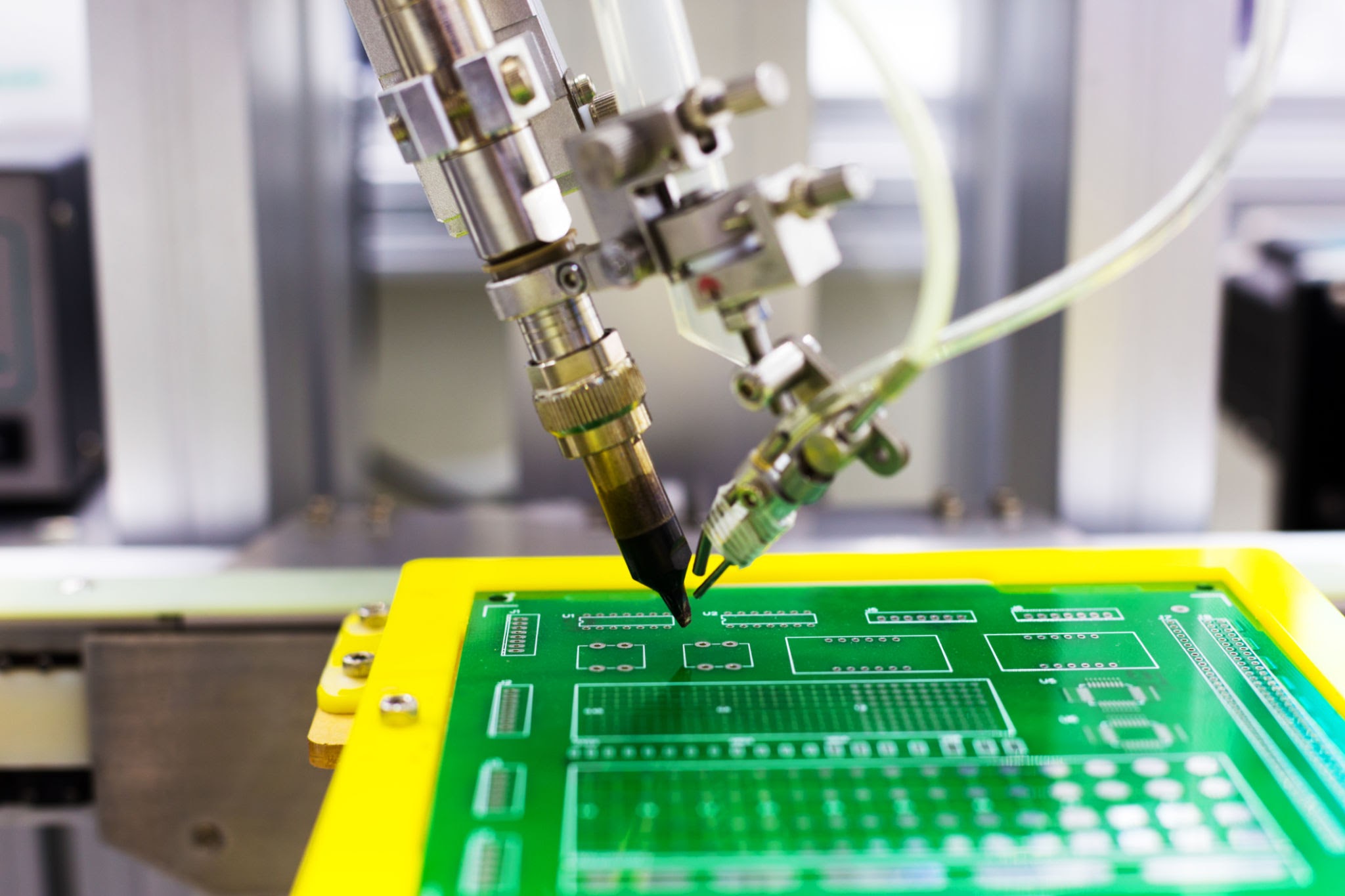
- Solder Paste Printing Machine:
- Purpose: Solder paste printing machines deposit solder paste onto PCBs before component placement.
- Detailed Workflow:
- Place a stencil over the PCB with openings corresponding to solder pad locations.
- Apply solder paste over the stencil.
- A squeegee spreads the solder paste evenly across the stencil.
- Excess solder paste is scraped away, leaving only paste in the stencil openings.
- Remove the stencil, leaving solder paste on the PCB.
- Key Components: Stencils, squeegees, alignment systems.
- Recommended URL: Solder Paste Printing Overview
- Pick and Place Machine:
- Purpose: Pick and place machines automatically position surface-mount components onto PCBs.
- Detailed Workflow:
- The vision system identifies component positions on feeders.
- Robotic arms with vacuum nozzles pick up components from the feeders.
- The machine accurately places components onto the PCB based on programmed coordinates.
- Components are placed at high speeds, with vision systems ensuring precision.
- PCBs move through the machine, and components are placed in the desired locations.
- Key Components: Robotic arms, vision systems, feeders.
- Recommended URL: Pick and Place Machines
- Reflow Oven:
- Purpose: Reflow ovens melt solder paste to create solder joints between components and PCBs.
- Detailed Workflow:
- PCBs with solder paste and components enter the oven on a conveyor belt.
- The oven has multiple temperature-controlled zones.
- In the preheat zone, the temperature gradually rises to activate the flux in the solder paste.
- In the reflow zone, the solder paste reflows, forming solder joints.
- Cooling zones gradually reduce the temperature to solidify the solder joints.
- PCBs exit the oven with properly formed solder joints.
- Key Components: Heating elements, conveyor systems, temperature controllers.
- Recommended URL: Reflow Soldering Basics