Prototype Shield Kits are essential components used in the design and development of electronic prototypes. These kits consist of printed circuit boards (PCBs) with pre-designed layouts and components that can be easily assembled to create functional electronic circuits. Etching technology plays a vital role in the fabrication of these prototype shield kits by allowing for precise pattern transfer onto the surface of the PCBs.
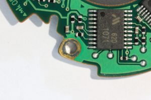 Etching technology offers several advantages in the production of Prototype Shield Kits. One of the key benefits is the ability to quickly and easily produce custom designs. With etching technology, designers can create their own customized layouts, and the etching process can be used to transfer the pattern onto the surface of the PCB with high accuracy and precision. This allows for rapid prototyping and design iteration, enabling designers to test and refine their designs quickly.
Another advantage of etching technology for Prototype Shield Kits is its ability to handle a wide range of materials. PCBs are made of various materials such as FR-4 fiberglass, aluminum, and copper, and each material has its unique properties. Etching technology can handle these different materials with ease, allowing for the production of customized components based on specific requirements.
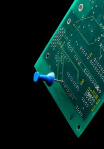 The etching process for Prototype Shield Kits involves several steps. The first step is the creation of a custom design using computer-aided design (CAD) software. The design is then transferred onto a special etching film, which is used to transfer the pattern onto the surface of the PCB. The PCB is then coated with a layer of photoresist material, and the etching film is placed onto the surface of the PCB. The PCB is then exposed to ultraviolet light, which hardens the photoresist layer in the areas not covered by the etching film. The etching film is then removed, and the PCB is etched using a chemical solution to remove the unwanted copper, leaving behind the desired circuit pattern.
 Etching technology offers several advantages in the production of Prototype Shield Kits. One of the key benefits is the ability to quickly and easily produce custom designs. With etching technology, designers can create their own customized layouts, and the etching process can be used to transfer the pattern onto the surface of the PCB with high accuracy and precision. This allows for rapid prototyping and design iteration, enabling designers to test and refine their designs quickly.
Another advantage of etching technology for Prototype Shield Kits is its ability to handle a wide range of materials. PCBs are made of various materials such as FR-4 fiberglass, aluminum, and copper, and each material has its unique properties. Etching technology can handle these different materials with ease, allowing for the production of customized components based on specific requirements.
 The etching process for Prototype Shield Kits involves several steps. The first step is the creation of a custom design using computer-aided design (CAD) software. The design is then transferred onto a special etching film, which is used to transfer the pattern onto the surface of the PCB. The PCB is then coated with a layer of photoresist material, and the etching film is placed onto the surface of the PCB. The PCB is then exposed to ultraviolet light, which hardens the photoresist layer in the areas not covered by the etching film. The etching film is then removed, and the PCB is etched using a chemical solution to remove the unwanted copper, leaving behind the desired circuit pattern.
Difference between traditional sheet metal precision processing VS Chemical etched sheet metal processing
VECO’s video to learn what metal etching is.
Comments related to etching technology:
From @chadr2604: There is another way it involves stacking many layers of very thin material with an There is another way it involves stacking many layers of very thin material with an adhesive, pressing the stack, then either stamping or punching the blank then heating it to release the adhesive. The parts will not be as accurate the tolerance is limited to about .002″ but if its good enough its much faster.
From @chadr2604: If you try to cut that stack with a laser you will just start a fire we had an aluminum fire trying that.Modern precision sheet metal fabrication includes a common technique known as etching, which differs from traditional sheet metal fabrication in several ways. Here are some key differences between etching and traditional precision sheet metal fabrication:
-
- Principle: Traditional sheet metal fabrication typically involves mechanical processes such as cutting, bending, and punching to shape and form metal sheets. Metal etching by Metal Etching Machine , on the other hand, is a chemical process that uses specialized etchants to selectively corrode the metal surface, achieving precise etched patterns and features.
- Accuracy and Complexity: Etching offers advantages in terms of precision and complexity. By controlling the composition, concentration, temperature, and etching time of the etchant, extremely fine etching can be achieved with accuracy down to sub-micron levels. Additionally, etching allows for the creation of intricate geometries, microstructures, and patterns that may be difficult to achieve using traditional mechanical methods.
- Processing Speed and Cost: Etching generally offers faster processing speeds, particularly in large-scale production. In comparison, traditional mechanical fabrication methods may require more time and cost to achieve the same level of precision and complexity.
- Materials Compatibility: Etching techniques are applicable to a range of metal materials, such as copper, aluminum, stainless steel, and titanium. Traditional sheet metal fabrication methods may have limitations when it comes to certain materials or thicker metal sheets.
- Design Flexibility: Etching provides greater design flexibility. By incorporating techniques like photolithography or screen printing during the etching process, complex patterns and structural designs can be achieved. This makes etching suitable for applications in microelectronics, optical devices, microfluidic devices, and more.
