In the realm of high-volume PCB manufacturing, advanced wet processing technologies play a crucial role in achieving both speed and precision. For industrial engineers and production managers, optimizing etching processes is key to maintaining efficiency and delivering high-quality PCBs at scale.
Automation in Chemical Etching Lines
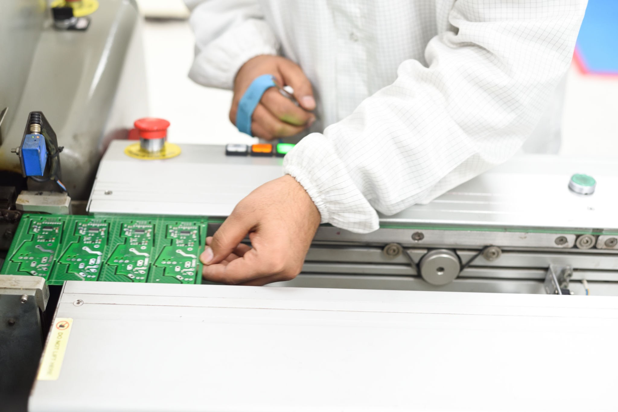
The move towards automation in chemical etching lines has drastically improved both speed and consistency in PCB manufacturing. Automated systems reduce human intervention, ensuring precise and repeatable results while minimizing the risk of errors. Automation also enhances throughput, making it ideal for high-volume production environments.
Robotic Panel Handling and Conveyor Systems
Robotic handling and conveyor systems are integral to automating the PCB etching process. These systems ensure that panels are consistently aligned and moved through the etching line without disruption. The use of robotics not only increases processing speed but also reduces labor costs and the risk of contamination due to manual handling.

| Feature | Benefits |
|---|---|
| Automation | Reduced human error and labor costs |
| Consistency | Ensures precise panel alignment |
| Speed | Accelerates throughput, ideal for high-volume production |
| Integration | Seamless with other etching and processing stages |
Closed-Loop Etchant Regeneration
In high-volume production, etchant regeneration is essential for reducing operational costs and environmental impact. Closed-loop systems continuously filter and regenerate etchant chemicals, ensuring they remain effective throughout the process. This not only cuts down on the need for fresh chemicals but also improves the quality and consistency of the etching process.
Precision Etching for Ultra-Fine Pitch Designs
With the increasing demand for high-density PCBs, precision etching is critical for producing ultra-fine pitch designs. Advanced etching machines, combined with precision control systems, can achieve etch widths of 20 microns or less, which is essential for modern applications like smartphones and medical devices.
Laser Direct Imaging (LDI) Integration
LDI-BM40 INLINE LDI-BM40 Series Laser Direct Imging System
Laser Direct Imaging (LDI) has revolutionized PCB etching by enabling direct imaging of fine features onto photoresist-coated copper. LDI allows for incredibly precise patterning, which is crucial for achieving the required performance in high-density PCBs.

| Technology | Advantages |
|---|---|
| Laser Imaging | High precision with no contact, reducing defects |
| High Resolution | Enables ultra-fine features for complex designs |
| Reduced Setup Time | No need for photomasks, faster production cycles |
Microetching for Blind/Buried Vias
Microetching techniques are essential for blind and buried vias, which are increasingly common in multi-layer PCBs. By applying precise chemical etching to these small vias, manufacturers can ensure that the vias are electrically conductive while maintaining the structural integrity of the PCB.
Reducing Waste in High-Volume Operations
Reducing waste is crucial for cost efficiency in high-volume PCB manufacturing. Innovations in waste management, such as etchant recovery and neutralization systems, have helped manufacturers minimize material waste while also meeting environmental regulations.
Etchant Recovery and Neutralization Systems
Etchant recovery systems help reduce the need for constant replenishment of etchant chemicals, improving operational efficiency. Neutralization systems treat the spent etchant, rendering it safe for disposal or reuse. These systems not only save money but also contribute to sustainability efforts by reducing chemical waste.
| System | Benefit |
|---|---|
| Etchant Recovery | Reduces consumption of chemicals |
| Neutralization | Complies with environmental regulations |
| Cost-Efficiency | Lowers overall production costs |
Energy-Efficient Heating/Cooling Units
Energy-efficient heating and cooling units are another critical component of high-volume PCB manufacturing. These units maintain optimal temperatures during the etching process while minimizing energy consumption. This contributes to both cost savings and environmental sustainability.
Case Study: Automotive PCB Manufacturing
The automotive industry demands the highest standards in PCB manufacturing. Automotive PCBs require precision, reliability, and the ability to withstand harsh environments. By integrating advanced etching technologies, manufacturers have been able to meet the rigorous performance and safety standards set by the industry.

One notable case is a leading automotive PCB supplier that implemented closed-loop etchant systems and robotic handling to achieve consistent quality in high-volume production runs. These systems allowed the company to lower production costs while ensuring that each PCB met the strict requirements for automotive applications.
For more insights into automotive PCB manufacturing, refer to IPC Automotive Standard.
Meeting IPC-6012 Standards for Reliability
The IPC-6012 standard defines the quality and reliability of printed circuit boards. For mass production, adhering to these standards is non-negotiable. Advanced etching technologies, including precision etching and etchant regeneration, help manufacturers meet the stringent requirements for electrical performance and mechanical durability. Ensuring compliance with IPC-6012 guarantees that the PCBs are fit for high-performance applications.
Emerging Trends: Additive vs. Subtractive Processes
The debate between additive and subtractive processes is heating up in PCB manufacturing. Subtractive etching has long been the industry standard, but additive techniques, such as direct inkjet printing of copper traces, are gaining traction. Additive processes offer more flexibility and can be more efficient for smaller production runs, while subtractive processes remain the go-to for large-scale, high-precision etching.
Semi-Additive Processing (SAP) for Miniaturization
One emerging trend in PCB manufacturing is semi-additive processing (SAP), which combines elements of both additive and subtractive processes. SAP allows for the creation of ultra-fine traces with high precision, making it ideal for miniaturized designs and applications where space and performance are critical.