All posts by droganetching

How acid etching machines acid etch metal parts

Acid etching, also known as photo etching, chemical etching or chemical milling, is a sheet metalworking technology which uses acid etchants to machine complex, highly accurate precision metal components.

Acid etching machines are used to remove material from metal parts using acid. The process involves the following steps:

  • Preparation: The metal part is cleaned thoroughly to remove any dirt, grease, or contaminants from the surface. This is important to ensure proper adhesion of the acid and uniform results.
  • Masking: Areas that should be protected from the acid are covered using a mask or a resist material. This could be done by applying a special adhesive film or using a resist pen to draw the desired pattern on the part.
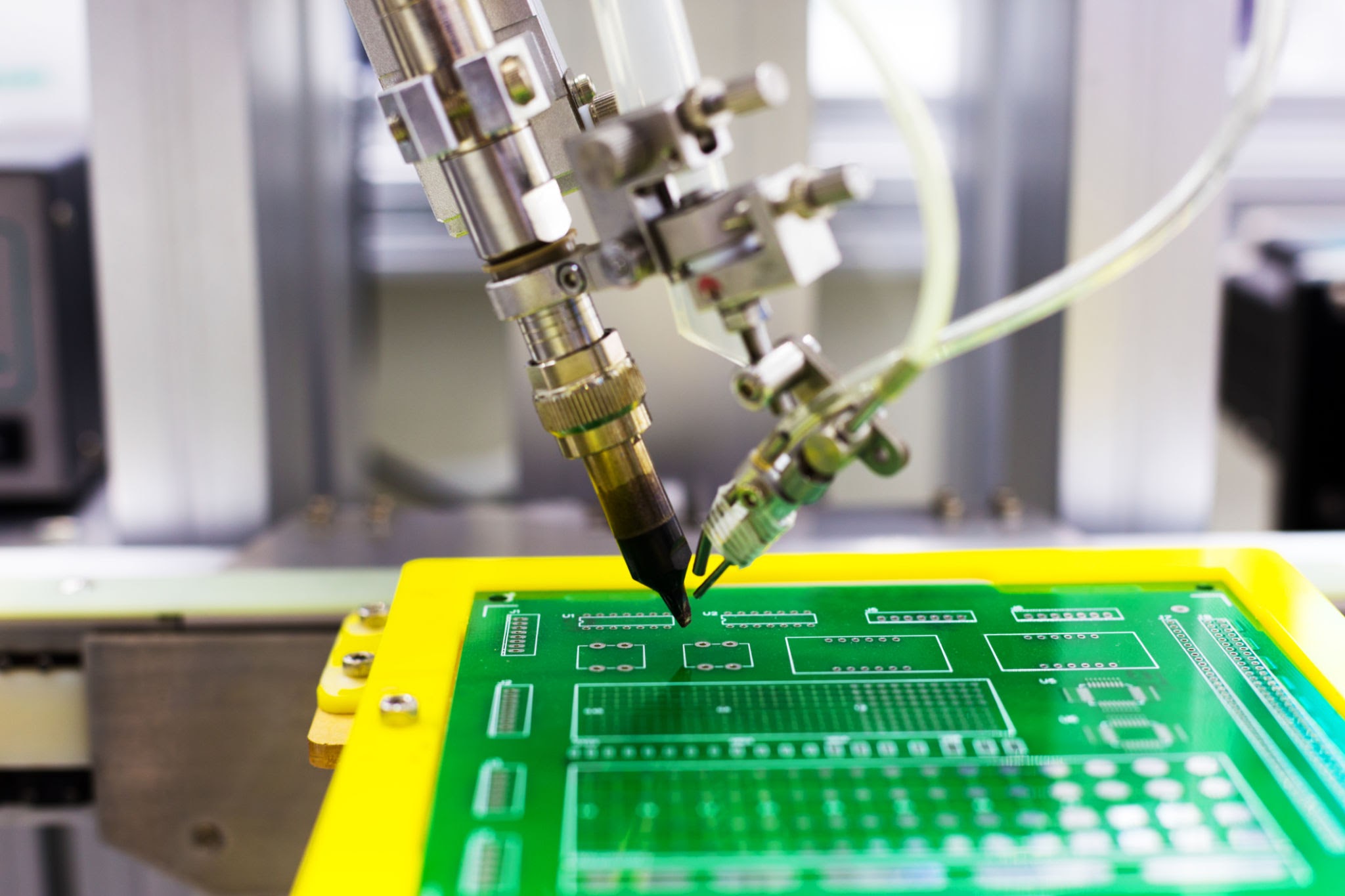
  • Acid application: The prepared metal part is then placed in the acid etching machine. The machine consists of a tank filled with a suitable acid solution such as ferric chloride or hydrochloric acid. The part is submerged in the acid solution, and the time and temperature are controlled depending on the desired depth and speed of etching.
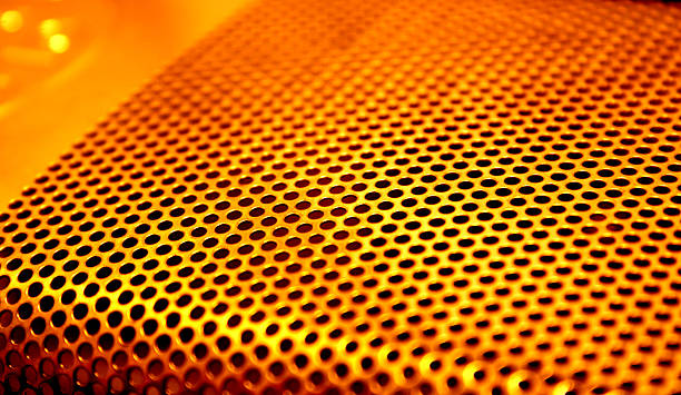
  • Etching process: The acid dissolves the exposed metal surface, creating a recessed pattern or design. The depth and quality of the etch can be controlled by adjusting the time, temperature, and concentration of the acid solution.
  • Rinsing and neutralizing: Once the desired etching is achieved, the metal part is removed from the acid solution and thoroughly rinsed with water to remove any residual acid. It is then neutralized using a neutralizing agent to stop the etching process and prevent further reaction with the metal.
  • Finishing: After the etching process, the resist material is removed, and the metal part is cleaned, dried, and polished if necessary. This reveals the etched pattern or design on the metal surface.

It is important to follow safety procedures and use appropriate protective equipment when working with acid

What does owning an acid etching machine do?

Owning an acid etching machine allows you to perform acid etching processes on metal parts at your own facility. This offers several benefits:

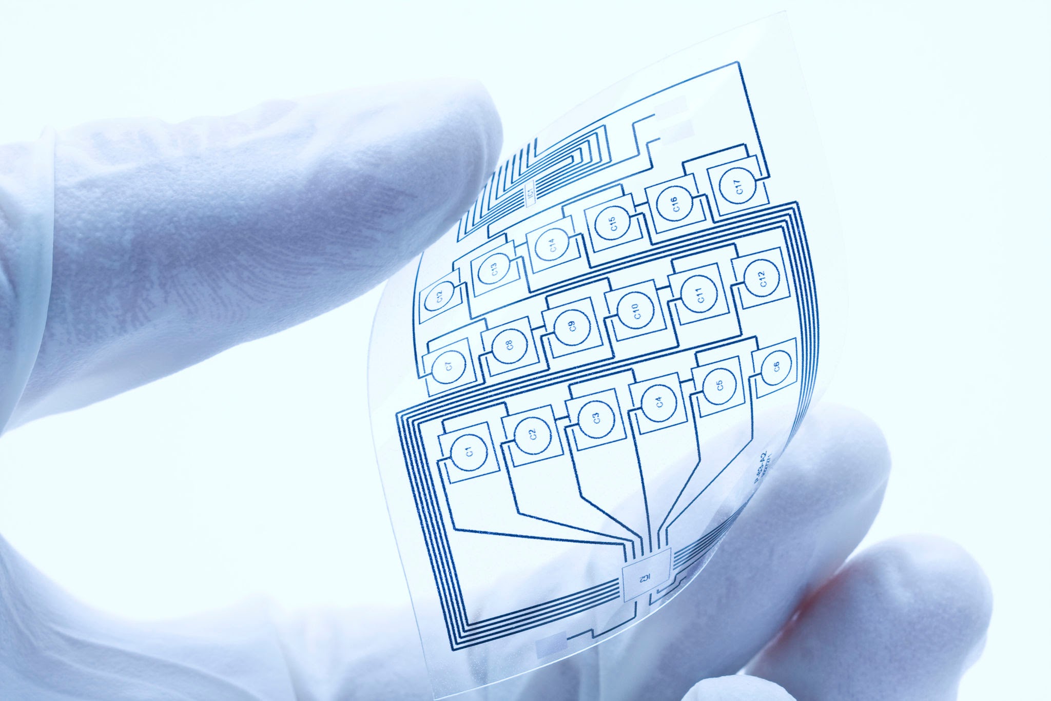
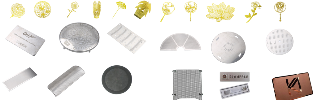
  1. Customization: With an acid etching machine, you have the freedom to customize metal parts according to your specific requirements. You can etch intricate designs, logos, serial numbers, or any desired patterns onto the metal surface. This allows for personalization and branding opportunities.
  2. Prototyping and product development: Acid etching machines enable you to quickly and efficiently create prototypes or test different designs on metal parts. This helps in the product development process by allowing you to evaluate aesthetics, functionality, and fit before committing to large-scale production.
  3. Production control: Owning an acid etching machine gives you control over the production process. You can etch metal parts in-house, ensuring quality control, shorter lead times, and reduced dependency on external suppliers. This can be particularly useful for businesses that require custom or small-batch production.
  4. Cost savings: By owning an acid etching machine, you can eliminate the need for outsourcing etching services, which can be costly and time-consuming. In the long run, this can lead to cost savings and improved efficiency.
  5. Versatility: Acid etching machines can be used on a wide range of metals, including stainless steel, aluminum, brass, copper, and more. This versatility allows you to work with different materials and expand your applications.

However, it is important to note that owning an acid etching machine also requires proper knowledge, training, and adherence to safety guidelines to ensure the safe handling and disposal of acids involved in the process.

What metals can an acid etcher etch?

  • Stainless steel: Acid etching can be used to create intricate designs, patterns, logos, or text on stainless steel surfaces, commonly used in the fabrication of kitchen appliances, automotive parts, and architecture.
  • Aluminum: Acid etching can be applied to aluminum surfaces to etch designs, text, or even photographs. It is commonly used in industries such as aerospace, signage, and decorative applications.
  • Brass: Brass can be etched using acid to create decorative patterns, logos, or designs. Acid etching on brass is often used in jewelry, nameplates, or decorative items.
  • Copper: Acid etching can be used on copper surfaces to create artistic designs, engravings, or patterns. It is commonly employed in the production of artworks, sculptures, and electrical components.
  • Nickel: Acid etching can be employed on nickel surfaces for various purposes, such as decorative elements, prototypes, or to create specific surface textures.
  • Zinc: Acid etching can be used on zinc surfaces to create intricate designs, textures, or patterns. It is often employed in architectural applications and the production of decorative items.

See all the metals our acid etchers can etch!

What do I need to know about acid-etched metal design?

  1. Assumptions Matter: Before delving into the design criteria, it’s crucial to set the right assumptions. For instance, in the case of wet etching, we assume a specific thickness. For the purpose of this discussion, let’s consider a thickness ranging from 0.1mm.
  2. Etching design formulas versus material thickness: Assuming a material thickness of 0.1mm, one of the first design criteria to consider is the hole diameter. To ensure proper etching, it’s often recommended to make the hole slightly larger than the material thickness. In this case, 1.2 times the material thickness would be 0.1mm * 1.2 = 0.12mm. Therefore, if the material thickness is 0.1mm, the hole should be designed to have a diameter of at least 0.12mm.
  3. Material Choice: The choice of material plays a significant role in wet etching. Different materials react differently to etchants. Engineers must select materials that are compatible with the chosen etchant to ensure a successful process.
  4. Hole Size Matters: The size of the holes created during wet etching is a critical design criterion. Smaller holes may lead to incomplete material removal, while larger holes may compromise structural integrity. Typically, materials with a thickness of 100μm or less can accommodate holes with a diameter of 0.12mm or more. Larger holes often result in more aesthetically pleasing and structurally sound outcomes.
  5. Alignment and Precision: Achieving precise alignment of the etched features is vital. Design drawings should incorporate alignment markers or registration features to ensure accurate positioning during the etching process. This is particularly crucial when dealing with multilayer structures or when specific patterns must be aligned with pre-existing features.
  6. Minimum Feature Size: It’s advisable to establish a minimum feature size for your design drawings. For instance, it’s generally recommended that no marked details be smaller than 0.1mm. This corresponds to 100μm. Maintaining a minimum feature size helps ensure that the etching process can accurately replicate the desired patterns and structures without the risk of incomplete or distorted etching.
  7. Quality Control and Inspection: Design criteria should include provisions for quality control and inspection during and after the wet etching process. This involves specifying methods and tools for verifying that the final product meets the intended design specifications. Inspection processes may include optical microscopy, surface profilometry, or other measurement techniques to validate critical dimensions and surface finish.

Customize Your Acid Etcher from Dragon Etching

    Wet Film Precision Metal Etching Process and Machine

    Wet film etching is another key technique in the precision metal etching process, offering an alternative approach to achieving fine patterns and features on thin metal substrates.

    1. Substrate Preparation:

    • Just like in dry film etching, the process begins with a clean metal substrate. The substrate is typically cleaned to remove any contaminants, ensuring proper adhesion of the photoresist layer.

    2. Application of Photoresist:

    • Instead of dry film resist, wet film etching utilizes a liquid photoresist. The photoresist is applied to the metal substrate by various methods such as spin coating, dip coating, or spray coating. It forms a thin, uniform layer over the entire surface.

    3. Soft Baking:

    • After the photoresist is applied, it undergoes a soft baking process. This step involves heating the substrate to remove solvent and to ensure the photoresist adheres well to the metal surface.

    4. Exposure to UV Light:

    • A photomask or phototool is used to project a specific pattern onto the photoresist-coated substrate. The exposed areas of the photoresist become chemically altered and become either more or less soluble depending on the type of photoresist used.

    5. Development:

    • The substrate is then immersed in a developer solution. The developer removes the soluble regions of the photoresist, revealing the underlying metal surface in a pattern that corresponds to the exposed areas of the photoresist.

    6. Etching:

    • The substrate, with the developed photoresist pattern, is immersed in an etching solution, which chemically removes the exposed metal areas. The etching solution can be an acid or alkaline solution depending on the specific metal being etched. Similar to dry film etching, the etchant selectively dissolves the metal while leaving the protected areas covered by the photoresist untouched.

    7. Rinsing and Inspection:

    • After etching, the substrate is thoroughly rinsed to remove any remaining etchant and residual photoresist. The etched features are inspected for accuracy and quality at this stage.

    8. Stripping of Photoresist:

    • The photoresist is typically removed after etching. This can be done using a solvent that dissolves the photoresist without affecting the etched metal features.

    9. Additional Processing (Optional):

    • Depending on the specific application, additional processes such as passivation, plating, or other post-etch treatments may be applied to the metal substrate to enhance its properties or protect it from environmental factors.

    10. Final Inspection and Quality Control: – The finished metal component undergoes a final inspection to ensure that the etched features meet the required specifications and quality standards. This may involve measurements, visual inspections, and other quality control procedures.

    Wet film etching offers many of the same advantages as dry film etching, including high precision, customization, and compatibility with various metal substrates. However, it has its own set of considerations and requirements, such as the need for liquid photoresists and precise control of the coating and soft baking processes. Wet film etching is commonly used in industries that require intricate metal components and where the flexibility of using liquid photoresists is beneficial.

    Wet film etching, as an alternative to dry film etching, possesses several distinctive features and advantages, making it suitable for specific applications.

    • Homogeneous Coating Thickness:
      • Wet film etching allows for the deposition of a highly uniform and consistent photoresist layer on the metal substrate. This results in even etching across the entire surface, reducing variations and defects in the final product.
    • Excellent Adhesion:
      • Liquid photoresists can offer strong adhesion to metal substrates, ensuring that the resist adheres firmly during the etching process. This helps maintain the integrity of the mask pattern and prevents delamination.
    • Variety of Photoresists:
      • Wet film etching can use a wide range of photoresist types, including positive and negative photoresists, each with its own characteristics. This versatility allows for the selection of the most suitable resist for the specific application.
    • Versatile Substrate Compatibility:
      • Wet film etching is compatible with various metals and alloys, similar to dry film etching. This versatility enables manufacturers to choose the material that best suits their requirements.
    • Multi-Layer Etching:
      • In some cases, wet film etching can be used for multi-layer etching processes where different metals or materials are etched sequentially, allowing for complex component manufacturing.
    • High Aspect Ratio Etching:
      • Wet film etching can achieve high aspect ratio features, meaning it is capable of etching deep, narrow channels or holes in metal substrates. This is crucial for certain microfabrication applications and MEMS devices.
    • Controllable Etching Rate:
      • The etching rate in wet film etching can often be precisely controlled by adjusting parameters such as etchant concentration, temperature, and agitation. This control is important for achieving specific etching depths or feature dimensions.
    • Rapid Prototyping:
      • Wet film etching is suitable for rapid prototyping and small-batch production, providing a quicker turnaround time compared to some other metal fabrication methods.
    • Minimal Tool Wear:
      • Since wet film etching is a chemical process, it does not involve physical tooling or machining. Consequently, there is no tool wear, which can be advantageous for maintaining consistent quality over time.
    • Environmental Considerations:
      • Similar to dry film etching, wet film etching is generally considered environmentally friendly as it does not produce significant hazardous waste or emissions, particularly when using environmentally friendly developer and etchant solutions.
    • Integration with Other Processes:
      • Wet film etching can be easily integrated into larger manufacturing processes, making it compatible with subsequent steps such as plating, passivation, or additional patterning steps.
    • Quality Control and Inspection:
      • Wet film etching, like dry film etching, allows for rigorous quality control and process monitoring, ensuring that final components meet specified tolerances and standards.
    Photo Chemical Machining Process
    Wet Film Precision Metal Etching Process and Machine Video

    Wet Film Precision Metal Etching Process:

    Equipment:

    • Coater for Wet Film Resist:
      • Purpose: Used to evenly apply a wet film resist onto the metal surface.
    • Drying Oven:
      • Purpose: Dries the wet film resist after application, ensuring proper adhesion and consistency.
    • UV Exposure Unit:
      • Purpose: Exposes the dried wet film resist to UV light through a photomask, creating a pattern on the resist.
    • Developer:
      • Purpose: Contains a chemical solution that removes the unexposed portions of the wet film resist, revealing the metal surface beneath.
    • Etching Machine:
      • Purpose: Selectively removes metal from the exposed areas using chemical etching solutions, creating the desired pattern.
    • Stripping Machine:
      • Purpose: Removes any remaining wet film resist from the metal surface after etching.

    Workflow:

    • Metal Cleaning:
      • Clean the metal sheet or component to remove impurities and contaminants.
    • Wet Film Resist Application:
      • Place the metal sheet or component in the coater.
      • Apply the wet film resist evenly onto the cleaned metal surface. This resist is typically a liquid that covers the entire surface.
    • Drying:
      • Transfer the metal with the applied wet film resist to a drying oven.
      • The oven dries the resist, evaporating any solvents and ensuring that the resist adheres properly to the metal.
    • Exposure:
      • Place the metal with the dried wet film resist under the UV exposure unit.
      • Expose the resist to UV light through a photomask that carries the desired pattern. The UV light cures the resist in the exposed areas, making it resistant to etching.
    • Development:
      • Transfer the exposed metal to the developer.
      • The developer contains a chemical solution that dissolves the unexposed portions of the wet film resist, revealing the metal surface underneath. This reveals the pattern for etching.
    • Etching:
      • Immerse the metal into the chemical etching machine containing the etching solution.
      • The chemical selectively removes the exposed metal areas, leaving the protected areas intact. Etching continues until the desired depth or pattern is achieved.
    • Rinsing and Cleaning:
      • Rinse the metal thoroughly with water or a suitable rinse solution to remove etching chemicals and residues.
    • Stripping (if needed):
      • Use a stripping machine or stripping chemicals to remove any remaining wet film resist from the metal surface. This step ensures a clean, finished product.
    • Final Inspection:
      • Inspect the etched metal for quality, accuracy, and adherence to specifications.
      • Any necessary post-processing or quality control checks are performed at this stage.

    The wet film precision metal etching process is suitable for applications where fine details and intricate patterns are required. It offers an alternative to dry film etching and is commonly used in industries such as electronics, microfabrication, and precision engineering.

    If you are interested in finding out about Wet Film Metal Etching Equipment overall price. Please do not hesitate to contact us. Usually we will contact you within 2 days after we receive your information.

      Dry Film Precision Metal Etching Process and Machine

      Dry film etching is a crucial step in the precision metal etching process, which is a highly precise and controlled technique for creating intricate patterns and features on thin metal sheets or foils. This process is often used in various industries, including electronics, aerospace, medical devices, and more, where precision and accuracy are paramount.

      Here are some additional features and aspects to consider about dry film etching:

      • High Precision and Accuracy:
        • Dry film etching is known for its exceptional precision and accuracy. It can create intricate and finely detailed patterns with tolerances as tight as a few micrometers. This level of precision is essential for manufacturing components used in electronics and other high-tech applications.
      • Cost-Effective for Prototyping and Small Production Runs:
        • Dry film etching is well-suited for prototyping and small production runs. Unlike some other manufacturing processes that require expensive tooling or molds, dry film etching is more cost-effective for producing small quantities of complex metal parts.
      • Customization and Design Flexibility:
        • Design changes can be implemented relatively easily in the dry film etching process. Since it involves exposing a resist to a mask, altering the mask design allows for rapid changes in the final etched pattern. This flexibility is advantageous when designing custom components.
      • Material Compatibility:
        • Dry film etching is compatible with various metals and alloys, including stainless steel, copper, aluminum, and more. This versatility allows manufacturers to choose the material that best suits the application’s requirements.
      • No Tool Contact:
        • Unlike some traditional machining processes that involve physical tooling, dry film etching is a non-contact method. This eliminates the risk of tool wear and damage to the substrate, making it ideal for delicate or thin materials.
      • Minimal Heat Generation:
        • Dry film etching is a cold-etching process, meaning it does not generate significant heat during the etching stage. This lack of thermal stress minimizes the risk of material distortion or warping, which is particularly important for thin metal foils.
      • Burr-Free and Stress-Free Etching:
        • The process produces burr-free edges and stress-free parts. This is crucial for components used in sensitive applications like microelectronics and medical devices, where sharp edges or residual stress can be problematic.
      • Scalability:
        • Dry film etching can be scaled up for larger production volumes when needed. This scalability makes it adaptable for both small-scale and large-scale manufacturing.
      • Environmental Considerations:
        • Dry film etching is generally considered to be a more environmentally friendly process compared to some other metal fabrication methods, as it does not produce large quantities of hazardous waste or emissions.
      • Quality Control and Process Monitoring:
        • Due to its precision, dry film etching allows for robust quality control and process monitoring. Manufacturers can closely monitor each step of the process to ensure that the final components meet the required specifications.
      • Wide Range of Applications:
        • Dry film etching is used in diverse industries, including electronics for printed circuit boards (PCBs), microelectromechanical systems (MEMS), sensors, medical devices, aerospace components, and more. Its versatility makes it applicable in various fields.

      Overall, dry film etching is a highly specialized and valuable manufacturing process that excels in producing precise, intricate metal components while offering flexibility and cost-effectiveness for both small-scale and large-scale production.

      Dry Film Metal Etching Equipment:

      • Metal Cleaning Machine:
        • Purpose: Used to clean the metal surface, removing contaminants to ensure proper adhesion of the dry film resist.
      • Pressure Layer Machine:
        • Purpose: Precisely applies the dry film resist onto the metal surface, ensuring uniform adhesion and thickness.
      • Exposure Machine:
        • Purpose: Exposes the dry film resist to UV light through a photomask, creating a pattern on the resist.
      • Developer:
        • Purpose: Contains a chemical solution that removes the unexposed portions of the dry film resist, revealing the metal surface beneath.
      • Etching Machine:
        • Purpose: Selectively removes metal from the exposed areas using chemical etching solutions, creating the desired pattern.
      • Stripping Machine:
        • Purpose: Removes any remaining dry film resist from the metal surface after etching.
      Photo Chemical Machining Process
      Precision Metal Etching Process Video

      Dry Film Metal Etching Workflow:

      • Metal Cleaning:
        • Clean the metal sheet or component to remove impurities and contaminants.
      • Pressure Layer:
        • Apply the dry film resist onto the cleaned metal surface using the pressure layer machine. Ensure uniform adhesion and thickness.
      • Exposure:
        • Place the metal with the dry film resist under the exposure machine.
        • Expose the resist to UV light through a photomask that carries the desired pattern.
      • Development:
        • Transfer the exposed metal to the developer, which removes the unexposed resist, exposing the metal underneath.
      • Etching:
        • Immerse the metal into the chemical etching machine containing the etching solution. The chemical selectively removes the exposed metal areas, leaving the protected areas intact.
      • Rinsing and Cleaning:
        • Rinse the metal thoroughly to remove etching chemicals and residues.
      • Stripping (if needed):
        • Use stripping chemicals to remove any remaining masking material (resist) from the metal surface.
      • Final Inspection:
        • Inspect the etched metal for quality and accuracy.

      If you are interested in finding out about Dry Film Metal Etching Equipment overall price. Please do not hesitate to contact us. Usually we will contact you within 2 days after we receive your information.

        Machines for high-precision metals production processes

        Photo Chemical Machining Process
        Equipment required for precision metal processing

        Precision Metal Etching Process: The Precision Metal Etching Process is a sophisticated manufacturing method used to selectively remove metal from thin sheets or foils with high accuracy, creating intricate and precise patterns.

        • Photoresist Application Machine:
          • Purpose: Applies a uniform layer of photoresist onto metal sheets for protection and pattern transfer.
          • Detailed Workflow:
            • Load clean, flat metal sheets or foils onto the machine’s conveyor system.
            • A precision dispensing system applies a uniform layer of photoresist onto the metal surface.
            • The coated metal sheets are transported through a drying mechanism to ensure even and complete drying.
        • Photomask Alignment System:
          • Purpose: Ensures accurate alignment of photomasks with metal sheets for precise pattern transfer.
          • Detailed Workflow:
            • Metal sheets with photoresist are aligned with photomasks using precision optical or mechanical alignment systems.
            • The alignment system ensures that the photomask is accurately positioned over the metal sheet to transfer the desired pattern during exposure.
        • UV Exposure Unit:
          • Purpose: Exposes the photoresist to UV light, hardening it and protecting it from etching.
          • Detailed Workflow:
            • The aligned metal sheets and photomasks are exposed to UV light in a controlled environment.
            • The UV light hardens the photoresist in areas not covered by the photomask, effectively creating a protective mask on the metal surface.
        • Chemical Etching Machine:
          • Purpose: Selectively removes metal from exposed areas of the metal sheets to create the desired pattern.
          • Detailed Workflow:
            • Metal sheets with hardened photoresist are immersed in a chemical etchant bath.
            • The etchant reacts with and dissolves the unprotected metal, leaving behind the desired pattern.
            • The etchant bath’s temperature, concentration, and agitation are carefully controlled for precise etching.
            • The etching process is closely monitored to achieve the desired depth and precision.
        • Rinsing and Drying Station:
          • Purpose: Removes residual etchant and ensures clean, dry metal components.
          • Detailed Workflow:
            • After etching, metal sheets are carefully removed from the etchant bath.
            • The sheets are rinsed in clean water to remove any remaining etchant.
            • A drying mechanism, such as hot air or infrared heating, thoroughly dries the metal sheets.
        • Quality Inspection Equipment:
          • Purpose: Verifies the accuracy and quality of the etched metal components.
          • Detailed Workflow:
            • Precision measurement tools, optical inspection systems, and quality control checks are employed to ensure that the etched components meet required specifications.
            • Measurements are taken to confirm dimensional accuracy, and optical inspections verify the quality of the etched pattern.

        Manufacturer Recommendation: For precision metal etching services, one highly regarded manufacturer is DragonEtching. They offer the following advantages:

        • Extensive Experience: DragonEtching has over 50 years of experience in precision metal etching, making them a trusted industry leader.
        • Advanced Technology: They utilize state-of-the-art photochemical etching processes and equipment to ensure high precision and quality.
        • Customization: DragonEtching specializes in custom etching solutions, allowing for intricate and complex patterns tailored to customer specifications.
        • Quality Assurance: The company is ISO 9001:2015 certified, demonstrating their commitment to quality and precision.
        • Diverse Materials: DragonEtching can etch a wide range of materials, including copper, stainless steel, and more.

        Recommended Guide to Machines for Printed PCB Production Processes

        It is unbelievable that these devices are needed to manufacture a PCB board.#machine #manufacture
        PCB production process and the equipment used
        • PCB Etching Machine: From Dragon Etching
          • Purpose: PCB etching machines are used to selectively remove unwanted copper from the surface of a copper-clad board to create the desired circuit pattern.
          • Process:
            • The PCB is first cleaned to remove any contaminants.
            • A layer of photoresist is applied to the board’s surface.
            • A photomask, containing the desired circuit pattern, is aligned and placed on the board.
            • The board is exposed to UV light, which hardens the photoresist in areas not covered by the mask.
            • The etching machine sprays an etchant (e.g., ferric chloride) onto the board, which dissolves the exposed copper, leaving behind the circuit traces.
            • After etching, the remaining photoresist is stripped to reveal the clean copper traces.
          • Key Components: The machine includes a conveyor system for transporting boards, nozzles for uniform etchant distribution, and chemical control systems to monitor and control the etching process parameters like temperature, flow rate, and immersion time.
        • PCB Cleaning Machine: From Dragon Etching
          • Purpose: PCB cleaning machines are essential for removing various contaminants and residues from the surface of printed circuit boards.
          • Process:
            • The PCB is placed on a conveyor system that passes it through a series of cleaning stages.
            • Typically, the first stage involves a pre-cleaning step to remove heavy contaminants.
            • Subsequent stages employ ultrasonic cleaning baths, chemical cleaning agents, and brushes or nozzles to thoroughly clean the board’s surface.
            • Rinse cycles follow to remove cleaning agents and residues.
            • Drying mechanisms, such as hot air or infrared heating, ensure the board is completely dry.
          • Key Components: These machines consist of conveyor belts, cleaning tanks, brushes or nozzles for cleaning agents, drying mechanisms, and filtration systems to maintain the cleanliness of cleaning solutions.
        • PCB Developing Machine: From Dragon Etching
          • Purpose: PCB developing machines are used to develop the exposed photoresist on a PCB, revealing the circuit pattern.
          • Process:
            • The PCB is loaded onto a conveyor or rack system.
            • It is then passed through a developer bath that contains a developer solution (typically alkaline) which removes the unexposed photoresist.
            • The time of immersion and the temperature of the developer solution are carefully controlled to achieve the desired development.
            • After developing, the board is rinsed to remove any residual developer.
          • Key Components: Key components include developer baths, conveyor systems, and temperature control units for precise process control.
        • PCB Stripping Machine: From Dragon Etching
          • Purpose: PCB stripping machines are used in semiconductor manufacturing to remove photoresist or other unwanted layers from wafers.
          • Process:
            • The machine can use chemical processes, such as wet etching or solvent stripping, or mechanical methods, like abrasive brushing, to remove the unwanted layers.
            • The choice of method depends on the specific application and material to be stripped.
          • Key Components: Components may include chemical tanks, spray nozzles, and mechanical components for stripping, as well as exhaust systems to handle chemicals safely.
        • PCB Grinding Machine: From Dragon Etching
          • Purpose: PCB grinding machines are used in semiconductor manufacturing to grind and polish silicon wafers for flatness and smoothness.
          • Process:
            • Wafers are mounted on a rotating chuck.
            • Abrasive materials (such as diamond grinding wheels) are used to remove material from the wafer’s surface.
            • Precision control systems ensure uniform grinding and polishing.
          • Key Components: Key components include the rotating chuck, abrasive materials, and precision control systems for grinding parameters.
        • PCB Through-Hole Plating: From Dragon Etching
          • Purpose: Through-hole plating machines are used in PCB manufacturing to add a metal layer to through-holes in a printed circuit board, creating a conductive path.
          • Process:
            • The PCB is first cleaned and prepared.
            • It is then immersed in an electroplating bath containing a metal solution (typically copper).
            • An electrical current is applied to deposit the metal layer inside the through-holes.
            • After plating, the board is rinsed and dried.
          • Key Components: Components include electroplating baths, cathodes, anodes, and control systems for regulating plating parameters, as well as rinse and drying stations.
        • PCB Drilling Machine: From Dragon Etching
          • Purpose: PCB drilling machines create holes for component leads and vias in printed circuit boards.
          • Detailed Workflow:
            1. Load the PCB onto the machine’s worktable.
            2. Program the CNC control system with coordinates for the holes to be drilled.
            3. Select the appropriate drill bits based on hole size requirements.
            4. The machine’s high-speed spindle begins drilling holes according to the programmed coordinates.
            5. Automatic tool changes may occur if different hole sizes are needed.
            6. Once all holes are drilled, the PCB is removed from the machine.
          • Key Components: Precision drill bits, CNC control system, worktable.
        • PCB Routing Machine (PCB Router):
          • Purpose: PCB routing machines trim excess PCB material and separate individual boards from a larger panel.
          • Detailed Workflow:
            1. Load the PCB onto the routing machine.
            2. Program the CNC control system with the desired cutting paths.
            3. The machine’s rotating routing bits follow the programmed paths, precisely cutting the PCB.
            4. As each PCB is cut from the panel, it is moved to a separate collection area.
          • Key Components: Routing bits, CNC control software, worktable.
          • Recommended URL: PCB Routing Techniques
        • Solder Paste Printing Machine:
          • Purpose: Solder paste printing machines deposit solder paste onto PCBs before component placement.
          • Detailed Workflow:
            1. Place a stencil over the PCB with openings corresponding to solder pad locations.
            2. Apply solder paste over the stencil.
            3. A squeegee spreads the solder paste evenly across the stencil.
            4. Excess solder paste is scraped away, leaving only paste in the stencil openings.
            5. Remove the stencil, leaving solder paste on the PCB.
          • Key Components: Stencils, squeegees, alignment systems.
          • Recommended URL: Solder Paste Printing Overview
        • Pick and Place Machine:
          • Purpose: Pick and place machines automatically position surface-mount components onto PCBs.
          • Detailed Workflow:
            1. The vision system identifies component positions on feeders.
            2. Robotic arms with vacuum nozzles pick up components from the feeders.
            3. The machine accurately places components onto the PCB based on programmed coordinates.
            4. Components are placed at high speeds, with vision systems ensuring precision.
            5. PCBs move through the machine, and components are placed in the desired locations.
          • Key Components: Robotic arms, vision systems, feeders.
          • Recommended URL: Pick and Place Machines
        • Reflow Oven:
          • Purpose: Reflow ovens melt solder paste to create solder joints between components and PCBs.
          • Detailed Workflow:
            1. PCBs with solder paste and components enter the oven on a conveyor belt.
            2. The oven has multiple temperature-controlled zones.
            3. In the preheat zone, the temperature gradually rises to activate the flux in the solder paste.
            4. In the reflow zone, the solder paste reflows, forming solder joints.
            5. Cooling zones gradually reduce the temperature to solidify the solder joints.
            6. PCBs exit the oven with properly formed solder joints.
          • Key Components: Heating elements, conveyor systems, temperature controllers.
          • Recommended URL: Reflow Soldering Basics

        Photochemical Etching Service Specialists

        We are a dedicated team of experts specializing in Photochemical Etching services and manufacturing. In this blog, we’ll introduce you to our state-of-the-art facilities, highlight the capabilities of our Photochemical Etching machine, delve into the metals we can etch, explore precision levels, and discuss why Dragon Etching stands out among the competition.

        Learn about photochemical processes in one video

        Photo Chemical Machining Process
        The Photo Chemical Machining process has 9 essential steps to achieve simple or complex thin-metal components of one to one million parts. This is a very economical option for research and development or prototype phase of a project when quick turnaround is vital. Our PCM process is used to etch through metal thicknesses between .0005″ to .060″ and between .060″ to .250″ for depth etching on metal only.

        Our Cutting-Edge Facilities

        At Dragon Etching, we take pride in our cutting-edge laboratory facilities. These facilities are equipped with the latest technology and machinery that allow us to achieve the highest standards of precision and efficiency in Photochemical Etching. Our team of skilled professionals operates in an environment that fosters innovation and excellence, ensuring that every project meets the most stringent quality standards.

        Comprehensive Photochemical Etching Process

        It’s widely recognized that to complete the entire etching process, a variety of equipment is required in addition to the photochemical etching machine. At Dragon Etching, we offer two different combinations of photochemical services, each tailored to specific needs:

        Option 1: Using Dry Film  what is dry film etching?

        1. Cleaning Link: The cleaning process is crucial to remove any contaminants, ensuring a clean surface for subsequent steps. It prepares the material for the photoresist application.
        2. Lamination Link: In the lamination step, a dry film photoresist is applied to the cleaned substrate. This photoresist acts as a protective layer during the etching process, defining the areas that will remain after etching.
        3. Exposure Link: During exposure, the substrate with the dry film photoresist undergoes a precise exposure to UV light. This step transfers the desired pattern onto the photoresist.
        4. Developing Link: In the developing process, the exposed photoresist is developed, leaving behind the patterned areas. Unexposed areas are removed, revealing the underlying material.
        5. Etching Link: Etching is where the actual material removal occurs. The substrate is exposed to etching chemicals, which selectively remove material according to the pattern defined by the photoresist.
        6. Stripping Link: After etching, the remaining dry film photoresist is removed, leaving you with the final etched product.

        Option 2: Using Wet Film what is wet film etching?

        1. Cleaning Link: Similar to the dry film process, the cleaning step is essential to prepare the substrate by removing contaminants.
        2. Lamination Link: In this step, a wet film photoresist is applied to the substrate, forming a protective layer for subsequent processes.
        3. Exposure Link: The substrate with the wet film photoresist is exposed to UV light, creating the desired pattern on the photoresist.
        4. Developing Link: After exposure, the photoresist is developed, revealing the patterned areas on the substrate.
        5. Etching Link: Etching, as before, is where the material is selectively removed according to the pattern defined by the photoresist.
        6. Stripping Link: Finally, the remaining wet film photoresist is stripped away, leaving behind the finished etched product.

        At Dragon Etching, we offer both dry and wet film processes to cater to a wide range of project requirements. Our state-of-the-art facilities and experienced team ensure that each step of the process is executed with precision and efficiency, resulting in high-quality products for our clients.

        Dragon Etching’s Photochemical Etching Machine

        Our flagship Photochemical Etching machine is a marvel of engineering. Here are some key features that set it apart:

        • Unmatched Precision: The etching precision of our machine is an astonishing 0.018mm, enabling us to manufacture micro-sized components with unparalleled accuracy. This level of precision is a game-changer for industries that demand intricate designs and fine details.
        • Enhanced Efficiency: Our Photochemical Etching machine automates the intricate and time-consuming process of removing copper from PCBs. It’s capable of handling large volumes of boards in a shorter time, significantly increasing production efficiency. This means quicker turnaround times for your PCB orders.
        • Consistent Precision: The machine offers high accuracy and repeatability, ensuring consistent results and minimizing errors. It can achieve fine circuit traces and complex designs that may be challenging to accomplish manually.
        • Reduced Production Time: With faster etching speeds and automated processes, our machine significantly reduces overall production time. This not only saves time but also optimizes resource utilization and improves profitability.

        Metals Suitable for Photochemical Etching

        While copper Photochemical Etching is the most common, our expertise extends to several other metals, including:

        • Stainless Steel: Ideal for applications requiring corrosion resistance.
        • Nickel Alloys: Suitable for high-temperature and corrosive environments.
        • Aluminum: Perfect for lightweight designs and high-performance applications.
        • Titanium: Known for its lightweight yet robust properties.

        Learn more about photochemical etching materials

        Unrivaled Precision

        Our commitment to precision is unparalleled. Dragon Etching can achieve precision levels as fine as a few nanometers, making us the top choice for industries that demand the utmost precision in their projects. This level of accuracy opens up new possibilities for applications where precision is critical.

        Why Choose Dragon Etching?

        Dragon Etching stands out from other Photochemical Etching service providers in several key ways:

        • In-House Machine Manufacturing: We are not just a service provider; we also manufacture Photochemical Etching machines. Click here to learn about the Photochemical Etching Equipment Selection Guide. This unique capability allows us to offer customized solutions, tailored to your specific needs. Whether you need our services or a customized DIV Photochemical Etching Machine, we have you covered.
        • Advanced Laboratory Facilities: Our state-of-the-art laboratories are equipped with the latest machinery and technology, ensuring consistent and high-quality results for our clients.
        • Rapid Turnaround: We understand the importance of timely project completion. Our streamlined processes enable us to offer some of the fastest turnaround times in the industry, ensuring your projects are completed efficiently and on schedule.

        Exceptional Service Department Efficiency

        Our service department operates at peak efficiency, capable of achieving a remarkable output of up to 200 square meters of copper etching in a single day. This exceptional efficiency ensures that we can handle large-scale projects without compromising on quality.

        At Dragon Etching, precision, efficiency, and innovation are at the core of everything we do. Whether you require high-volume production or custom solutions, Dragon Etching is your trusted partner. Contact us today to experience the Dragon Etching difference firsthand.

        How do I select a photochemical etching service company if I need to use photochemical etching brass for a project right now?

        Experience and Expertise: Ensure that the company you choose has ample experience and expertise, particularly in dealing with brass. They should understand the characteristics of brass to effectively perform photochemical etching.
        Equipment and Technology: Familiarize yourself with the equipment and technology the company uses. Modern equipment often provides higher precision and efficiency. Ensure that their equipment and technology align with the requirements of your project.
        Quality Control: Inquire about the company’s quality control processes. They should have rigorous quality control standards to ensure your project meets the expected quality standards.
        Project Scale: Consider the scale of your project. Some companies may be better suited for large production batches, while others specialize in small batches or custom projects. Choose a company that fits the scale of your project.
        Delivery Time: Understand the company’s delivery times. If you have time constraints, ensure that the company can complete the project on schedule.
        Cost and Budget: Lastly, consider costs and your budget. Discuss project costs with the company and ensure it aligns with your budget.

        Essential Equipment for Opening a PCB Manufacturing Plant

        With the growing demand for electronic devices and technology, the need for printed circuit boards (PCBs) has skyrocketed. If you are considering venturing into the electronics manufacturing industry and want to open a PCB manufacturing plant, equipping your facility with the right tools is crucial for success. This article will guide you through the essential equipment required to set up a state-of-the-art PCB manufacturing plant.

        1. PCB Design Software:

        Before diving into production, you’ll need reliable PCB design software to create and optimize your circuit layouts. Numerous software options are available, ranging from user-friendly to advanced, offering various features like auto-routing, design rule checks (DRC), and schematic capture. Select a tool that suits your team’s proficiency and design complexity.

        1. CAM Software:

        Computer-Aided Manufacturing (CAM) software is essential to convert your PCB designs into machine-readable formats. This software ensures that the PCB manufacturing equipment understands and executes the design accurately during the production process.

        1. PCB Fabrication Equipment:

        a. CNC Machines (Drilling Machines): CNC (Computer Numerical Control) drilling machines are used to create holes for component placement and vias on the PCB. Choose machines that offer high precision and speed to streamline the manufacturing process.

        b. Etching Equipment: Etching is a crucial step in PCB manufacturing where unwanted copper is removed from the board surface. Acid etching and chemical-free methods (using plasma or lasers) are common techniques. Select the appropriate equipment based on your production scale and environmental concerns.

        c. Laminators: Laminators are used to apply dry film resist and copper layers onto the PCB substrate. This step is vital in creating the circuit pattern for subsequent etching.

        d. Exposure Units: Exposure units utilize UV light to transfer the PCB design’s image onto the photosensitive film or resist-coated board before etching. Consistent exposure is essential for high-quality PCBs.

        1. Soldering and Assembly Equipment:

        a. Pick-and-Place Machines: Automated Pick-and-Place machines accurately position and solder surface-mount components onto the PCB. These machines significantly enhance productivity and placement accuracy.

        b. Reflow Ovens: Reflow ovens are used to melt the solder and secure the components on the PCB during the soldering process. Proper temperature profiles are crucial to avoid defects.

        c. Wave Soldering Machines: For through-hole components, wave soldering machines are used to create solder connections simultaneously on multiple pins.

        1. Testing and Quality Control:

        a. Automated Optical Inspection (AOI) Systems: AOI systems perform visual inspections of assembled PCBs, identifying defects such as missing components, misalignment, or soldering issues.

        b. Flying Probe Testers: Flying probe testers are employed for functional testing of PCBs. They use movable probes to check connectivity and circuit performance.

        1. Environmental Controls and Safety Equipment:

        a. Cleanrooms: PCB manufacturing demands a dust-free and controlled environment. Cleanrooms ensure that airborne contaminants do not affect the quality of your boards.

        b. Safety Equipment: Ensure your employees have access to personal protective equipment (PPE) such as goggles, gloves, and face masks to guarantee their safety during manufacturing.

        It is unbelievable that these devices are needed to manufacture a PCB board.#machine #manufacture
        pcb production process

        PCB Equipment List

        Depart.ProcessEquipment
        PE EngineerFile InputFrontline InPlan Planning Software
        CAMOrbotech InCAM
        A/WOrbotech photo plotter
        Inner LayerInner FilmAutomatic Wet Film Coater
        Inner ExposureVarious manual and semi-auto exposure
        Inner Layer EtchUniversal DES( Develop-Etch-Strip) Lines
        AOI InspectionOrbotech Discovery, Camtek
        Brown OxideUniversal Alternative Oxide Line
        LaminatingBurkle, OEM, Heng-da Vacumm Presses
        DrillingMechnical DrillHitachi, Schmoll, HanStar
        Laser DrillMitsubishi Laser Drill
        Ourer LayerPlasma CleanReBorn RPP-V13
        PTHAutomatic Desmear and Electroless Copper
        Semi-Exposure5KW Manual Exposure
        LDI machineLaser Direct Imaging photeck
        Pattern PaltingAutomatic Panel Plating Line
        Automatic Pattern Plating Line
        MCP-PAL Vertical Continuous Plating Line
        Copper Via Fill Plating Tank
        Outer Layer EtchUniversal SES( Strip-Etch-Tin Strip) Line
        SM & MarkingSM PrintingHorizontal Semi Automatic Coater
        SM ExposureVarious SM Exposure
        LegendSprint 100
        Ourline CNCCNC Routers + CCD routers
        V-CutCNC V-score
        Punch DiePunch
        ChamferBevel
        Surface finishHASLTin/Lead HASL
        Leadfree HaslLead Free HASL
        ENIGUyemura
        ENEPIGSuccessful
        Imm. AgMacDermid(Planar)
        Imm. TinAtotech(Stannatech)
        ENTEKOSP
        Hard FGoldFull body gold, gold fingers and selective gold
        Flash GoldFull body and selevtive bondable soft gold
        Test & InspectionE-T Fixture2wire / 4wire Fxiture Test
        Flying Probe2wire / 4wire Flying Probe Test
        Reliability TestX-section and Microscopes, Impendence Test, High-Pot,
        Tg Test, Peel Strength, lonic Testing, IR Reflow, Thermal Chamber etc chrommotography,IST,CAF

        Mastering the Chemistry: Hydrofluoric Acid (HF) in PCB Wet Etching

        In the world of PCB manufacturing, precision and control are paramount in crafting intricate circuit patterns. One of the most potent and challenging chemical solutions utilized in the wet etching process is Hydrofluoric Acid (HF). Composed of hydrogen and fluorine, HF is a highly corrosive and hazardous acid known for its ability to dissolve various materials, including glass and metals. In this blog, we will delve into the specifics of Hydrofluoric Acid (HF) and provide valuable details on its technique for use in PCB wet etching machines, emphasizing safety and precision.

        In the field of chemistry Hydrofluoric Acid belongs to which category?

        Inorganic Fluxes

        Inorganic fluxes are highly corrosive, and are comprised of inorganic acids and salts such as hydrochloric acid, hydrofluoric acid, stannous chloride, sodium or potassium fluoride, and zinc chloride. These fluxes are capable of removing oxide films of ferrous and nonferrous metals such as stainless steel, Kovar and nickel irons, which cannot be soldered with weaker fluxes.

        Inorganic fluxes generally are used for nonelectronics applications such as the brazing of copper pipes. They are, however, sometimes used for lead-tinning applications in the electronics industry. Inorganic fluxes should not even be considered for electronics assemblies (conventional or surface mount) because of potential reliability problems. Their major disadvantage is that they leave chemically active residues than can cause corrosion and serious field failures.

        Performance criteria for chemical milling


        photoresists are in many ways more demanding than those of PWB fabricators; there is aplethora of different substrates such as Alloy 42,beryllium copper, iron-nickel alloys, molybdenum, tungsten, Invar, and many more. Theetching chemistries and etch conditions, which the resist must survive, are brutal. In addition to the more benign cupric chloride and the mainstream ferric chloride, you find mixtures of hydrofluoric and nitric acid which embrittle the resist, as well as very highly alkaline solutions of potassium ferrocyanide, which act like strippers on aqueous processable resists.

        What is Hydrofluoric Acid (HF)?

        Hydrofluoric Acid (HF) is a strong, colorless liquid acid with the chemical formula HF. Due to its reactivity and corrosiveness, HF is typically used with caution in specialized applications, such as glass etching, metal cleaning, and semiconductor manufacturing. In PCB wet etching, HF is employed to selectively remove silicon dioxide (SiO2) or glass passivation layers from semiconductor devices, enabling the creation of specific circuit patterns.

        Hydrofluoric Acid

        Technique of Using Hydrofluoric Acid (HF) for PCB Wet Etching:

        1. Preparing the HF Solution:

        To prepare the HF etchant solution, dilute the concentrated HF with deionized water to achieve the desired concentration. The concentration of HF is typically expressed in percentage (%). Common concentrations for PCB wet etching are around 5% to 10% HF.

        1. Personal Protective Equipment (PPE):

        Safety is paramount when handling HF. Always wear appropriate Personal Protective Equipment (PPE), including acid-resistant gloves, a full-face shield, chemical-resistant apron, and safety goggles to protect against splashes and inhalation of vapors.

        1. Proper Ventilation:

        Always work with HF in a well-ventilated area or under a fume hood to prevent exposure to its toxic and corrosive vapors.

        1. Etching Temperature:

        The etching temperature can significantly impact the etch rate and selectivity. Typically, HF etching is conducted at room temperature (around 20°C to 25°C) to ensure precision and consistency.

        1. Immersion Time:

        The immersion time in the HF etchant solution determines the depth of etching. Longer immersion times result in deeper etching, while shorter times yield shallower patterns. The immersion time should be carefully controlled based on the desired circuit design and the thickness of the SiO2 or glass passivation layer.

        1. Agitation:

        Gentle agitation of the etchant solution can promote an even distribution of the HF across the substrate’s surface, ensuring uniform and precise etching results.

        1. Neutralization and Disposal:

        HF should not be neutralized with alkaline substances, as this can produce toxic and corrosive fluoride salts. Instead, HF should be treated with specific HF neutralizing agents. After etching, the spent HF solution should be carefully collected and disposed of according to environmental regulations.

        Conclusion:

        Hydrofluoric Acid (HF) is a powerful tool in PCB wet etching, enabling engineers to achieve precision and control in crafting intricate circuit patterns. By adhering to proper safety protocols and technique, HF can be handled with confidence, and PCB manufacturers can create high-quality and reliable electronic devices. Embrace the chemistry of HF, and elevate your PCB manufacturing process to new heights of accuracy and excellence.

        As a wet process engineer, mastering the use of Hydrofluoric Acid (HF) in PCB wet etching empowers you to create cutting-edge electronic devices with flawless circuitry, revolutionizing the world of technology. Happy etching!

        Unleashing the Potential of Ferric Chloride Etchant in PCB Wet Etching: A Comprehensive Guide

        In the realm of printed circuit board (PCB) manufacturing, the etching process plays a pivotal role in shaping intricate circuit patterns. Among the array of etchants available, Ferric Chloride Etchant stands out as a reliable and efficient solution. Composed of ferric chloride (FeCl3), this chemical marvel offers engineers unparalleled control and precision during wet etching. In this blog, we will delve into the specifics of Ferric Chloride Etchant and provide valuable tips for its effective utilization in PCB wet etching machines.

        What is Ferric Chloride Etchant?

        Ferric Chloride Etchant is an acidic solution containing ferric chloride, a potent chemical compound known for its exceptional ability to dissolve copper effectively. This unique etchant is widely employed in the PCB manufacturing industry for its excellent selectivity, allowing for the precise removal of copper from the PCB substrate without adversely affecting other materials.

        What Could Ideal Etch Factors Mean for SAP?

        If somehow you could get both the regeneration of cupric chloride and the vertical sidewalls of powderless ferric chloride etching, I think we would see a dramatic change in the PCB industry. Currently, using the semi-additive process (SAP) is the most practical way to obtain fine features. However, if sideways etch can be efficiently inhibited in the etchants we use today (cupric chloride and alkaline cupric chloride), SAP may not even be necessary in most cases. If you are unfamiliar with SAP, it can be summarized as a process where a copper-plated panel undergoes a selective plating process to form desired features on top of the copper that was already present. Once the features are plated onto the base copper, that panel gets etched to remove the base copper, thus leaving behind only the features that were added. Finding a way around SAP would mean skipping many long and costly steps in the PCB fabrication process. Without requiring SAP to obtain fine features, PCB shops would require less plating equipment and fewer resources to perform plating (i.e., chemicals, trained personnel, time to plate, and operating space).

        Image from:https://www.pcb.iconnect007.com/index.php/article/133191/the-chemical-connection-the-etch-factor/133194/?skin=pcb

        The Technique of Using Ferric Chloride Etchant in PCB Wet Etching Machine:

        1. Etchant Preparation:

        To prepare the Ferric Chloride Etchant solution, dissolve ferric chloride crystals in water. The recommended ratio is typically one part ferric chloride to three parts water, by weight. Always add the ferric chloride slowly to the water while stirring, and ensure you work in a well-ventilated area with proper safety equipment.

        1. Temperature Control:

        Maintaining the etchant at the ideal temperature is vital for achieving consistent and accurate etching results. The recommended operating temperature for Ferric Chloride Etchant typically ranges from 35°C to 45°C (95°F to 113°F). Consider using a temperature-controlled wet etching machine to ensure precise regulation.

        1. Immersion Time:

        The etching time directly influences the depth of copper removal. Longer immersion times result in deeper etching, while shorter durations yield shallower patterns. The immersion time can vary depending on the desired circuit design and the thickness of the copper layer.

        1. Agitation:

        Proper agitation of the etchant solution is essential for promoting an even distribution of the etchant across the PCB surface. Adequate agitation prevents over-etching or under-etching, ensuring uniformity in the etching process.

        1. Neutralization and Disposal:

        After completing the etching process, neutralize the Ferric Chloride Etchant to deactivate it and render it safe for disposal. Utilize a neutralizing agent, such as sodium bicarbonate (baking soda), to neutralize the etchant solution before disposing of it responsibly according to environmental regulations.

        1. Safety Precautions:

        Ferric Chloride Etchant is corrosive and can cause skin and eye irritation. Always wear appropriate personal protective equipment (PPE), such as gloves and safety goggles, and work in a well-ventilated area to avoid exposure to fumes.

        Ferric Chloride Etchant is a powerful ally in the PCB wet etching process, offering precision, control, and efficiency. By following the proper technique for its preparation and usage, engineers can create intricate circuit patterns with confidence. Embrace the potential of Ferric Chloride Etchant, and elevate your PCB manufacturing process to new heights of accuracy and excellence.

        As a wet process engineer, your mastery of Ferric Chloride Etchant will undoubtedly contribute to the success of PCB manufacturing, ushering in a new era of advanced electronic devices with flawless circuitry. Happy etching!

        Mastering the Art of Cupric Chloride Etchant in PCB Wet Etching: A Step-by-Step Guide

        In the realm of printed circuit board (PCB) manufacturing, Cupric Chloride Etchant stands as a powerful ally in achieving precision and control during the wet etching process. This chemical solution, composed of cupric chloride (CuCl2), enables engineers to selectively remove copper from PCB substrates, shaping intricate circuit patterns. In this blog, we will delve into the specifics of Cupric Chloride Etchant and provide valuable tips for its effective utilization in PCB wet etching machines.

        What is Cupric Chloride Etchant?

        Cupric Chloride Etchant is an acidic solution containing cupric chloride, a chemical compound known for its ability to dissolve copper efficiently. This etchant is widely used in the PCB manufacturing industry for its excellent selectivity, allowing for precise copper removal without adversely affecting other materials on the PCB.

        Tips for Using Cupric Chloride Etchant in PCB Wet Etching Machine:

        1. Etchant Preparation:

        To prepare the Cupric Chloride Etchant solution, mix cupric chloride crystals with hydrochloric acid (HCl) in a proper ratio. The common ratio is approximately 100 grams of cupric chloride per 100 milliliters of concentrated hydrochloric acid. Always add the acid to the water slowly while stirring, and ensure you’re working in a well-ventilated area with proper safety equipment.

        1. Temperature Control:

        Maintaining the right temperature is crucial for achieving accurate etching results. The ideal operating temperature for Cupric Chloride Etchant typically ranges from 35°C to 50°C (95°F to 122°F). Consider using a temperature-controlled wet etching machine to ensure precise regulation.

        1. Immersion Time:

        The etching time is directly related to the depth of copper removal. Longer immersion times result in deeper etching, while shorter times yield shallower patterns. The immersion time can vary depending on the desired circuit design and the thickness of the copper layer.

        1. Agitation:

        Gentle agitation of the etchant solution can enhance the etching process by promoting even distribution. Proper agitation helps prevent over-etching or under-etching and ensures uniformity across the PCB surface.

        1. Neutralization and Disposal:

        After the etching process, neutralize the Cupric Chloride Etchant to ensure it is deactivated and rendered safe for disposal. Utilize a neutralizing agent, such as sodium carbonate (Na2CO3), to neutralize the etchant solution before disposing of it responsibly according to environmental regulations.

        1. Safety Precautions:

        Cupric Chloride Etchant is corrosive and toxic, requiring careful handling. Always wear appropriate personal protective equipment (PPE), work in a well-ventilated area, and follow proper safety protocols to avoid accidents and exposure to harmful fumes.

        About Cupric and Alkaline
        Together, these etchants are used in the majority of PCB etch shops, with alkaline being the most popular. To provide a baseline of how they work, their etch reactions along with their corresponding regeneration reactions, can be found in Table 1.

        One of the main reasons these two etchants are the most used is because of their regeneration capabilities. With regeneration, you increase the capacity of copper you can etch. It also helps keep the etch rate at a consistent value. To maintain mass production of PCBs, it is important to keep the etch rate steady but also high enough to maximize output. Since etch rate can greatly influence production rates, it is a major factor when comparing etchants.

        https://pcb.iconnect007.com/index.php/article/132406/the-chemical-connection-etchants-of-the-industrycupric-vs-alkaline/132409/?skin=pcb

        Etch Factor

        Another matter where alkaline etchant is highly favored is etch factor, the ratio of downward etch to sideways etch. Alkaline etchant offers the benefit of a 4-to-1 etch factor (meaning it etches downward four times as much as it etches sideways). Cupric provides a standard 3-to-1 etch factor (Figure 1).

        Image from:https://pcb.iconnect007.com/index.php/article/132406/the-chemical-connection-etchants-of-the-industrycupric-vs-alkaline/132409/?skin=pcb

        Alkaline etchant’s better etch factor opens the opportunity to maintain finer spaces and line widths when you are etching panels with thicker copper layers. Although alkaline can provide a great etch factor, a 4-to-1 ratio can only be obtained if the etchant is kept at its optimal condition, which is easier said than done.

        Mastering the art of Cupric Chloride Etchant in PCB wet etching opens the door to unparalleled precision and control in circuit pattern creation. By adhering to proper etchant preparation, temperature regulation, immersion time, and safety precautions, engineers can craft intricate PCB designs with confidence. Embrace the power of Cupric Chloride Etchant and elevate your PCB manufacturing process to new heights of accuracy and efficiency.

        In the realm of printed circuit board (PCB) manufacturing, Cupric Chloride Etchant stands as a powerful ally in achieving precision and control during the wet etching process. This chemical solution, composed of cupric chloride (CuCl2), enables engineers to selectively remove copper from PCB substrates, shaping intricate circuit patterns. In this blog, we will delve into the specifics of Cupric Chloride Etchant and provide valuable tips for its effective utilization in PCB wet etching machines.