All posts by droganetching

FPCB manufacturing process

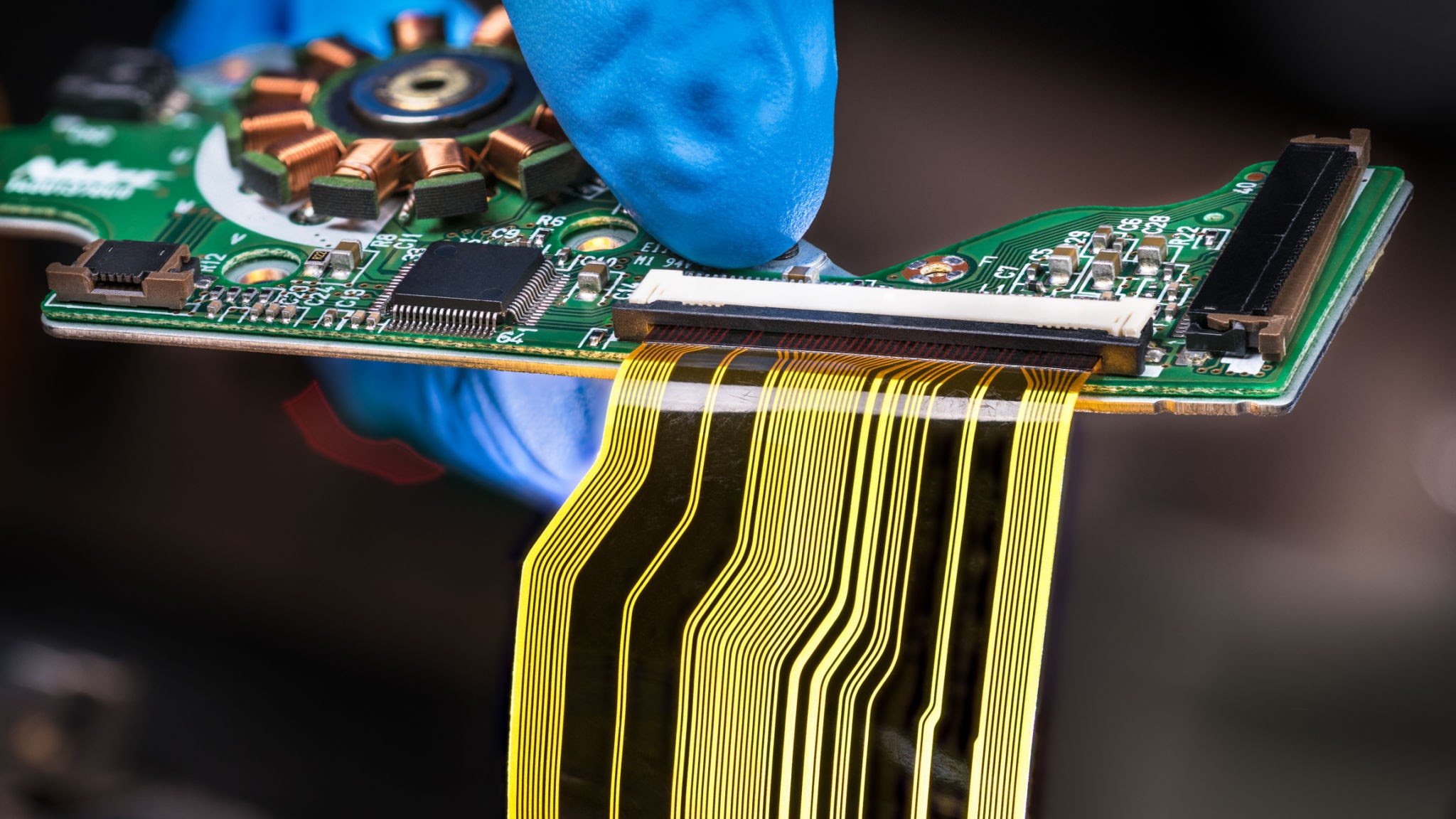
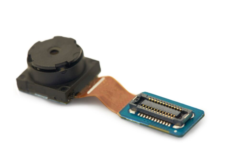
Flexible Printed Circuit Boards (FPCBs) are thin, flexible electronic circuits that are used in a wide range of applications, including smartphones, tablets, wearable devices, and automotive electronics. The manufacturing process for FPCBs involves several steps, including design, material selection, and fabrication.

  1. Design: The first step in FPCB manufacturing is designing the circuit layout. This involves determining the placement of components, the routing of traces, and any necessary connections or vias. Specialized software is used to create the circuit design.
  2. Material Selection: FPCBs are typically made of a flexible substrate material, such as polyimide or polyester film. The choice of material depends on the specific requirements of the application, including flexibility, temperature resistance, and durability.
  3. Copper Cladding: The flexible substrate is coated with a layer of copper on one or both sides. This is typically done through a process called electroless copper plating or electroplating, where a thin layer of copper is deposited onto the substrate surface.
  4. Imaging: A photosensitive material, called a photoresist, is applied to the copper-clad substrate. The circuit pattern is then transferred onto the photoresist using a photomask and exposure to ultraviolet light. This process allows for the creation of the desired copper traces and pads.
  5. Etching: After the imaging process, the exposed copper areas are etched away using an etching solution, leaving behind the desired circuit pattern. The photoresist is then removed, and the substrate undergoes a cleaning process to prepare it for the next step.
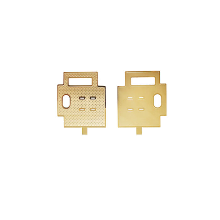
  6. Surface Finishing: Surface finishing techniques are employed to protect the exposed copper traces and pads and provide better solderability. Common surface finishes used in FPCB manufacturing include immersion gold, HASL (Hot Air Solder Leveling), and OSP (Organic Solderability Preservatives).
  7. Assembly: Once the FPCBs are fabricated, they can be assembled with electronic components. This involves placing the components onto the FPCB and soldering them in place. The assembly process can be performed using automated equipment or manual labor, depending on the complexity and volume of production.

Complete PCB Manufacturing Equipment: Single-Sided, Double-Sided, Multilayer, Rigid-Flex

Equip your facility with the comprehensive PCB manufacturing equipment needed to produce single-sided, double-sided, multilayer, and rigid-flex PCBs efficiently. Streamline your production process with the right tools. Get started today!

Single-Sided FPCB, Double-sided FPCB, Multilayer FPCB, and Rigid-Flex FPCB

To manufacture different types of flexible printed circuit boards (FPCBs), various equipment and processes are involved. Here’s a general overview of the equipment typically used for manufacturing single-sided FPCBs, double-sided FPCBs, multilayer FPCBs, and rigid-flex FPCBs:

  1. Single-Sided FPCB:
    • Substrate Cutting Machine: Used to cut the flexible substrate (usually polyimide or polyester) into desired shapes and sizes.
    • Imaging/Exposure Equipment: Used to transfer the circuit pattern onto the substrate through a photosensitive film or dry film resist.
    • Etching Machine: Used to chemically remove unwanted copper from the substrate, leaving behind the desired circuit pattern.
    • Plating Equipment: Used for copper electroplating to enhance the copper thickness and ensure good conductivity.
    • Solder Mask Coating Machine: Used to apply a protective solder mask layer over the copper traces, leaving only the desired areas exposed for soldering.
    • Surface Finishing Equipment: Used for applying a final finish to the exposed copper surfaces, such as hot air leveling (HASL), immersion gold, or immersion tin.
  2. Double-Sided FPCB:
    • Same equipment as for single-sided FPCBs, with the addition of the following:
    • Drilling Machine: Used to drill holes for component leads and vias to establish electrical connections between the two sides of the board.
    • Electroless Copper Deposition System: Used for depositing a thin layer of copper inside the drilled holes, forming the conductive vias.
  3. Multilayer FPCB:
    • Same equipment as for double-sided FPCBs, with the addition of the following:
    • Lamination Press: Used to bond multiple layers of flexible substrates together with adhesive layers.
    • Bonding Press: Used for bonding inner layers of the FPCB stack with copper foils.
    • Laser Drilling Machine: Used for high-precision drilling of microvias in the multilayer stack.
    • Copper Plating Line: Used for through-hole copper plating and subsequent copper buildup on the outer layers.
    • Additional Imaging/Exposure, Etching, and Plating Equipment: Required for the outer layer circuits.
  4. Rigid-Flex FPCB:
    • Same equipment as for multilayer FPCBs, with the addition of the following:
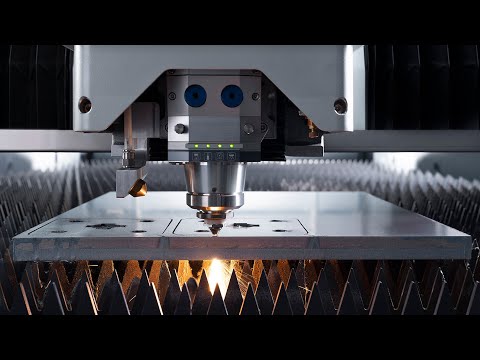
    • CNC Milling Machine: Used for precise cutting and shaping of the rigid sections.
    • Z-axis Registration System: Ensures accurate alignment between the rigid and flexible sections during lamination.
    • Additional Drilling and Plating Equipment: Required for the rigid sections.

Please note that specific equipment may vary depending on the manufacturer’s capabilities, technology requirements, and production scale. The above list provides a general idea of the equipment commonly used for manufacturing different types of FPCBs.

What equipment is required to produce single-sided FPCB, double-sided FPCB, Multilayer FPCB, and Rigid-Flex FPCB simultaneously?

If you want to produce single-sided FPCBs, double-sided FPCBs, multilayer FPCBs, and rigid-flex FPCBs simultaneously, you would need a comprehensive set of equipment that can handle the different manufacturing processes involved. Here’s an overview of the equipment you would typically require:

FPCB Manufacturing Machine

If you want to produce single-sided FPCBs, double-sided FPCBs, multilayer FPCBs, and rigid-flex FPCBs simultaneously, you would need a comprehensive set of equipment that can handle the different manufacturing processes involved. Here’s an overview of the equipment you would typically require:

  1. Substrate Cutting Machine: Used for cutting flexible substrates into desired shapes and sizes.
  2. Imaging/Exposure Equipment: Used for transferring circuit patterns onto the substrates using photosensitive films or dry film resists.
  3. PCB Etching Machine: Used for chemically removing unwanted copper from the substrates to form the circuit patterns.
  4. Plating Equipment: Used for copper electroplating to enhance copper thickness and conductivity.
  5. Solder Mask Coating Machine: Used for applying a protective solder mask layer over the copper traces.
  6. Surface Finishing Equipment: Used for applying final finishes to the exposed copper surfaces (e.g., HASL, immersion gold, or immersion tin).
  7. Drilling Machine: Used for drilling holes in the substrates for component leads and vias.
  8. Electroless Copper Deposition System: Used for depositing a thin layer of copper inside the drilled holes to create conductive vias.
  9. Lamination Press: Used for bonding multiple layers of flexible substrates together with adhesive layers in multilayer and rigid-flex FPCBs.
  10. Bonding Press: Used for bonding inner layers of the multilayer and rigid-flex FPCB stack with copper foils.
  11. Laser Drilling Machine: Used for high-precision drilling of microvias in the multilayer stack.
  12. CNC Milling Machine: Used for precise cutting and shaping of the rigid sections in rigid-flex FPCBs.
  13. Z-axis Registration System: Ensures accurate alignment between the rigid and flexible sections during lamination in rigid-flex FPCBs.
  14. Copper Plating Line: Used for through-hole copper plating and subsequent copper buildup on the outer layers in multilayer FPCBs.
  15. Additional Imaging/Exposure, Etching, and Plating Equipment: Required for producing the outer layer circuits in multilayer FPCBs.
  16. Additional Drilling and Plating Equipment: Needed for producing the rigid sections in rigid-flex FPCBs.

It’s important to note that producing all these types of FPCBs simultaneously would require a significant investment in equipment and may involve complex manufacturing processes. It’s advisable to consult with specialized PCB manufacturing equipment suppliers or industry experts to customize a production line that suits your specific requirements and budget.

Essential Machinery for PCB Production: Protection Act Compliance

The U.S. “Protection of Circuit Boards and Substrates Act” is a crucial piece of legislation that aims to safeguard the integrity and security of circuit boards and substrates used in various electronic devices. With the increasing demand for advanced electronic products, many businesses in the United States are considering expanding or building PCB production lines. In this blog, we will provide an interpretation of the Protection of Circuit Boards and Substrates Act, and delve into the essential machinery required in a PCB production line, including PCB etching machines, PCB cleaning machines, PCB drilling machines, PCB browning machines, PCB sandblasting machines, PCB polishing machines, PCB oxidation resistance machines, PCB desoldering machines, PCB stripping machines, and PCB developing exposing machines. This information will help visitors who are motivated to purchase these machines and establish or expand their own PCB production lines.

The “Protection of Circuit Boards and Substrates Act” is a significant legislation aimed at ensuring the security and integrity of circuit boards and substrates used in electronic devices within the United States. The act recognizes the critical role played by circuit boards and substrates in the functioning of electronic products and seeks to prevent unauthorized modifications, counterfeiting, and tampering that could compromise their performance or pose security risks.

The act encompasses various provisions and requirements that manufacturers, distributors, and users of circuit boards and substrates must adhere to in order to comply with the law. Some key aspects of the act include:

  1. Counterfeit Prevention: The act emphasizes the need to combat the production and distribution of counterfeit circuit boards and substrates. It prohibits the manufacturing, sale, or use of counterfeit components and mandates stringent measures to ensure the authenticity of these critical electronic parts.
  2. Traceability and Documentation: The act emphasizes the importance of traceability and documentation throughout the supply chain. Manufacturers and distributors are required to maintain detailed records of the origin, manufacturing process, and distribution of circuit boards and substrates. This information helps establish accountability and facilitates effective quality control and product recalls if necessary.
  3. Quality Assurance: The act promotes the implementation of rigorous quality assurance measures throughout the production process. Manufacturers are encouraged to adopt industry best practices and adhere to recognized standards to ensure the reliability, performance, and safety of circuit boards and substrates.
  4. Security Measures: The act recognizes the need to safeguard electronic devices against potential security threats. It encourages the use of secure designs, authentication mechanisms, and encryption technologies to protect the integrity of circuit boards and substrates. This is particularly relevant in applications where the confidentiality of data or critical operations are at stake.
  5. Compliance and Enforcement: The act establishes mechanisms for compliance verification and enforcement. Regulatory authorities are empowered to conduct inspections, audits, and investigations to ensure that manufacturers and distributors are in compliance with the provisions of the act. Non-compliance can result in penalties, fines, or other legal consequences.

The “Protection of Circuit Boards and Substrates Act” reflects the growing importance of circuit boards and substrates in today’s interconnected and technology-driven world. By establishing guidelines and regulations, the act aims to foster trust among consumers and businesses, protect intellectual property, and promote the safe and reliable use of electronic devices.

For businesses involved in the establishment or expansion of PCB production lines, understanding and adhering to the requirements outlined in the act is essential. Compliance with the act not only ensures legal adherence but also demonstrates a commitment to quality, security, and customer satisfaction.

The Protection of Circuit Boards and Substrates Act focuses on safeguarding the manufacturing, distribution, and use of circuit boards and substrates within the United States. The act imposes regulations to prevent counterfeiting, tampering, and unauthorized modifications to these critical components, ensuring the reliability and security of electronic devices. It is important for businesses engaged in PCB production to adhere to the requirements specified in this act to maintain compliance with the law and protect consumer trust.

Customized PCB production line for customers: A Customer Case Study #etching #cleaning #sandblasting
Dragon Etching Customized PCB production line for customers

Dragon Etching Essential Machinery in a PCB Production Line:

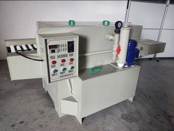
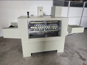
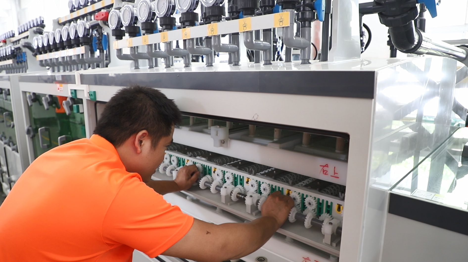
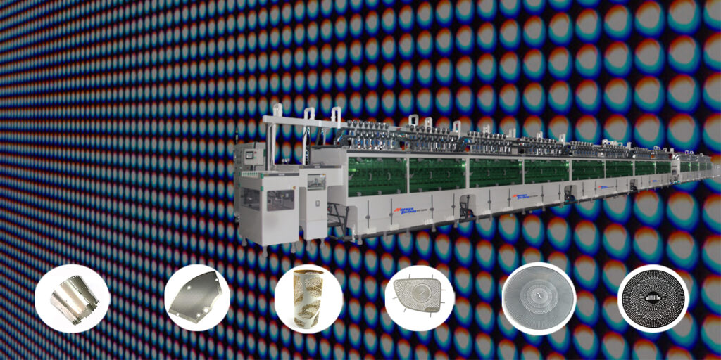
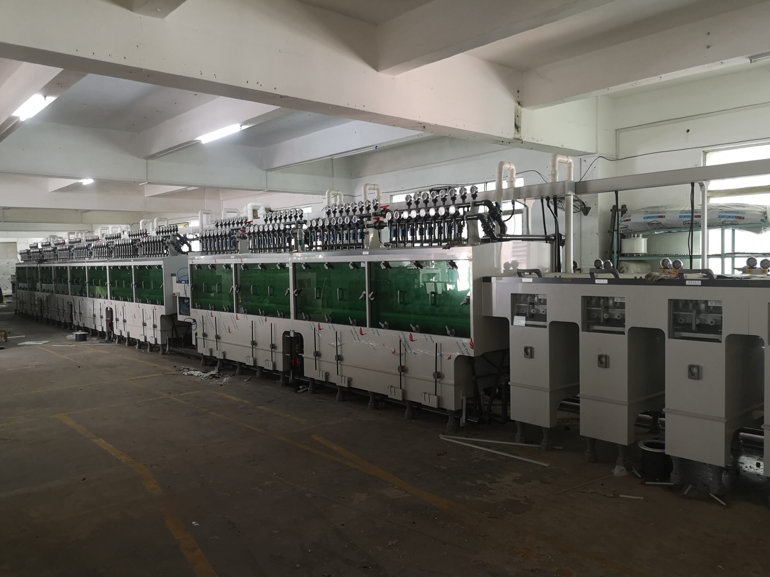
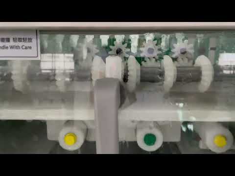
  • PCB Etching Machine: PCB etching machines are vital in the production process as they facilitate the removal of unwanted copper from the substrate, creating the desired circuitry. These machines use chemical processes to dissolve the excess copper, leaving behind the required copper traces for circuit connections.
  • PCB Cleaning Machine: PCB cleaning machines are used to remove any contaminants or residues that accumulate during the manufacturing process. They employ various cleaning methods such as ultrasonic cleaning, brush cleaning, and chemical cleaning to ensure the cleanliness and reliability of the circuit boards.
  • PCB Drilling Machine: PCB drilling machines are responsible for creating holes in the circuit boards to accommodate electronic components. These machines utilize high-speed rotating drill bits to accurately drill holes of varying sizes, ensuring precise placement and alignment.
  • PCB Browning Machine: PCB browning machines, also known as brown oxide machines, are used to create a protective layer on the exposed copper surfaces of the circuit boards. This layer prevents oxidation and enhances the conductivity of the copper traces, improving the overall performance and longevity of the PCB.
  • PCB Sandblasting Machine: PCB sandblasting machines are employed for surface preparation, primarily to remove solder mask or copper from specific areas. This process is crucial for creating solder pads and ensuring proper solder adhesion during component assembly.
  • PCB Polishing Machine: PCB polishing machines are used to refine the surface finish of circuit boards. They remove any imperfections, such as rough edges or burrs, resulting from the manufacturing process, and provide a smooth and uniform surface for further processing or component placement.
  • PCB Oxidation Resistance Machine: PCB oxidation resistance machines apply protective coatings to the circuit boards, safeguarding them against environmental factors such as humidity, moisture, and corrosive substances. These coatings enhance the reliability and durability of the PCBs, ensuring their longevity in demanding applications.
  • PCB Desoldering Machine: PCB desoldering machines are essential for repairing or reworking PCBs. They allow the removal of electronic components without damaging the board, enabling efficient repairs and replacements during the production process or after device assembly.
  • PCB Stripping Machine: PCB stripping machines are used to remove unwanted solder masks, ensuring accurate solder pad exposure

PCB Etching Machine Cleaning Solution

PCB etching machines are essential for manufacturing high-quality printed circuit boards (PCBs). Over time, these machines can become contaminated with chemicals and residue from the etching process, which can affect the quality of the etching and potentially damage the machine. To keep your PCB etching machine in top condition, regular cleaning is essential. In this article, we will discuss some tips for using a cleaning solution to clean your PCB etching machine.

  1. Selecting the Right Cleaning Solution: There are several types of cleaning solutions available for cleaning PCB etching machines. It is important to choose a cleaning solution that is safe for the machine and effective at removing the contaminants. Always refer to the manufacturer’s guidelines and recommendations when selecting a cleaning solution.
  2. Protecting Yourself: Before using the cleaning solution, ensure that you are wearing appropriate personal protective equipment (PPE), such as gloves, eye protection, and respiratory protection, if necessary. Cleaning solutions can be corrosive and hazardous, so it is essential to follow proper safety precautions.
  3. Preparing the Solution: Once you have selected a suitable cleaning solution, prepare it according to the manufacturer’s instructions. Typically, the solution will need to be diluted with water to achieve the desired concentration. Use distilled or deionized water, as tap water may contain impurities that can affect the cleaning process.
  4. Cleaning the Machine: To clean the PCB etching machine, apply the cleaning solution to a cloth or sponge and gently wipe down the surfaces. Pay particular attention to areas that are prone to contamination, such as the etching tank, nozzles, and pipes. Avoid using abrasive materials or scrubbers that could damage the machine.
  5. Rinsing and Drying: After cleaning the machine with the solution, rinse the surfaces thoroughly with clean water to remove any remaining residue. Use a clean cloth or paper towel to dry the machine and remove any excess water. It is essential to ensure that the machine is completely dry before using it again, as moisture can cause corrosion and damage to the machine.

In conclusion, cleaning your PCB etching machine with a suitable cleaning solution is essential for maintaining the quality of your PCBs and prolonging the life of your machine. By following these tips, you can help ensure that your machine is clean, safe, and functioning optimally, producing high-quality PCBs that meet your specifications and requirements.

PCB using a chemical solution

PCBs (Printed Circuit Boards) are essential components of modern electronic devices, providing a platform for connecting and controlling the various components and circuits that make up the device. PCBs are typically manufactured using a chemical process that involves etching the copper traces and pads on the board using a chemical solution. While this process is generally safe and effective, there are some cautions that should be taken when handling and working with the chemicals involved.

Choose the right etching solution: There are several different types of etching solutions available, each with its own properties and advantages. Some of the most commonly used etching solutions include ferric chloride, ammonium persulfate, and sodium persulfate. Before selecting an etching solution, consider the type of PCB you are manufacturing, the desired trace widths and depths, and the cost and availability of the solution.

Ventilation: The PCB etching process can produce harmful fumes and vapors, which can be toxic if inhaled in large quantities. It is essential to work in a well-ventilated area, preferably with an exhaust hood or other ventilation system, to prevent the buildup of fumes and vapors.

Cleanliness: PCBs must be thoroughly cleaned after the etching process to remove any residual chemicals and prevent contamination. Use a suitable cleaning solution and ensure that all equipment, tools, and surfaces are cleaned regularly to maintain a safe and clean working environment.

Dilution: Etching solutions are typically used in a diluted form, as the concentrated solution can be too aggressive and damage the board. It is essential to dilute the solution correctly, following the manufacturer’s instructions and using the correct ratio of solution to water. Be sure to use distilled or deionized water, as tap water may contain impurities that can affect the etching process.

Temperature: The temperature of the etching solution can have a significant impact on the etching process, affecting the speed and quality of the etch. Most etching solutions work best at a specific temperature range, typically between 35°C and 50°C. Use a thermometer to monitor the temperature of the solution and adjust as needed to maintain the desired temperature.

Agitation: Agitation of the etching solution is important for ensuring an even and consistent etch. This can be achieved by using an agitation system, such as a pump or bubbler, or by manually agitating the solution using a stirring rod. Ensure that the agitation is not too strong, as this can damage the board, or too weak, as this can result in uneven etching.

Safety measures: It is essential to follow proper safety procedures when working with PCB etching chemicals. Store the chemicals in a secure location away from children and pets, and dispose of them properly in accordance with local regulations. Avoid mixing different chemicals or using them in unintended ways, as this can cause dangerous reactions.

Safety: Etching solutions are corrosive and can cause skin and eye irritation, respiratory problems, and other health issues if not handled properly. Always wear protective gear, such as gloves, goggles, and a respirator, when handling etching solutions. Store the solutions in a secure location away from children and pets, and dispose of them properly in accordance with local regulations.

By following these etching solution usage tips, you can help ensure a successful and safe etching process, resulting in high-quality PCBs that meet the required specifications and performance standards.

The Advantages of Rigid Flex PCB – Production Process, Uses, and Top Manufacturers

rigid flex pcb

Learn about the benefits of using rigid flex PCBs, including their production process and use cases such as fingerprint technology. Discover top manufacturers and the equipment required for production.

igid-flex PCBs, also known as hybrid PCBs, are a combination of rigid and flexible circuit boards that are interconnected by plated through-holes. These circuit boards offer a variety of advantages over traditional PCBs, including increased reliability, reduced weight and space requirements, and enhanced design flexibility. In this article, we’ll explore the advantages of rigid-flex PCBs, their production process, and some of their common applications.

What is Rigid Flex PCB?

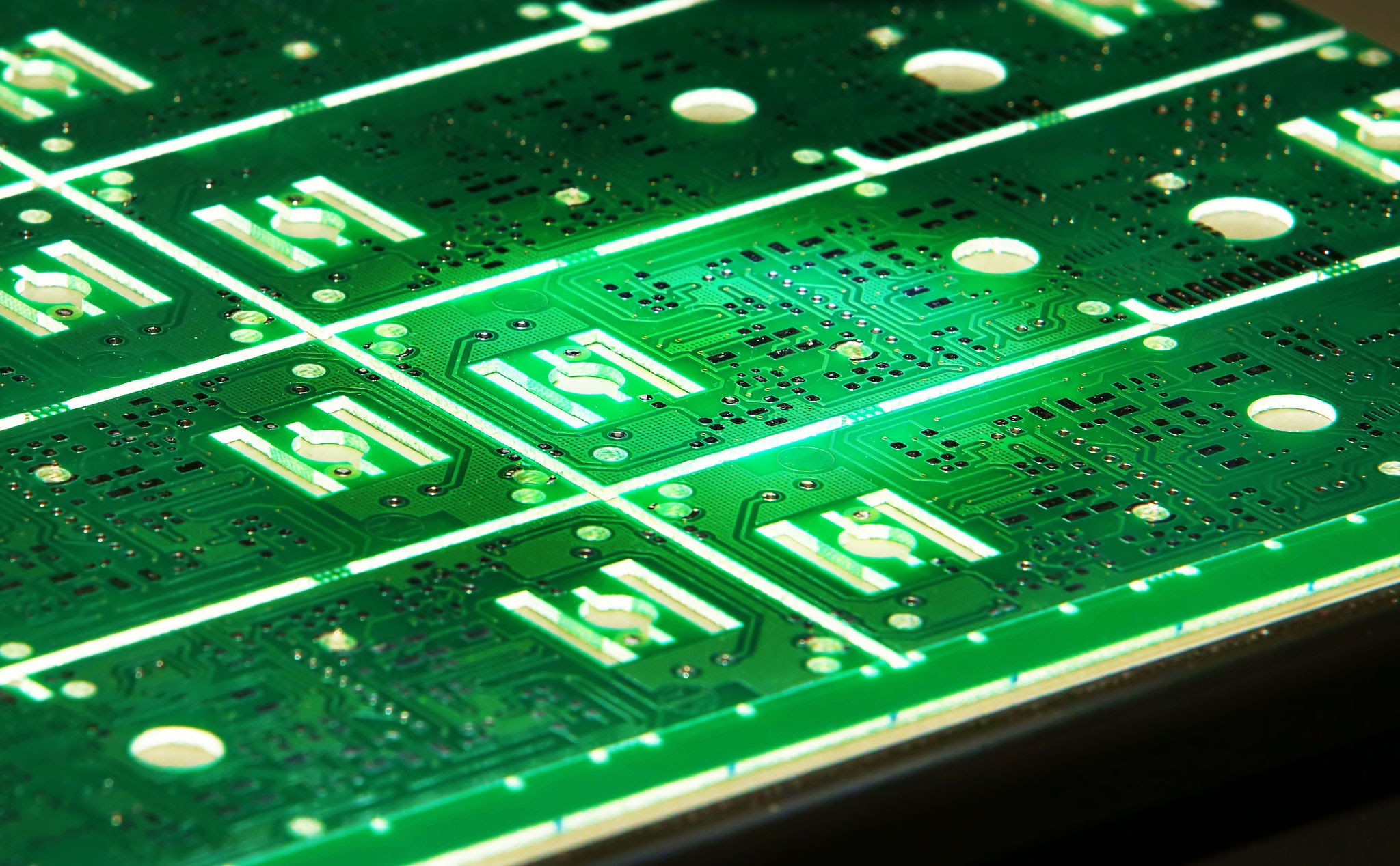
Rigid-flex PCBs are a type of printed circuit board that combines the characteristics of rigid and flexible circuits into a single design. These boards consist of multiple layers of flexible circuitry, which are laminated together with layers of rigid circuitry. The flexible sections of the board are typically used to connect components, while the rigid sections are used to mount components and provide mechanical stability.

Advantages of Rigid-Flex PCBs:

  1. Increased Reliability: The flexibility of these circuit boards makes them less susceptible to damage from mechanical stresses, vibration, and thermal expansion, which can improve their reliability.
  2. Reduced Weight and Space Requirements: The use of flexible circuitry can reduce the overall weight and size of the board, making them ideal for use in portable devices and other applications where space is limited.
  3. Enhanced Design Flexibility: The use of flexible circuitry also allows for more complex and intricate designs, which can improve performance and reduce manufacturing costs.
  4. Improved Signal Integrity: The use of flexible circuitry can reduce the number of interconnects required, which can improve signal integrity and reduce the potential for interference.
  5. Cost-Effective: Despite their many advantages, rigid-flex PCBs can be produced at a cost that is comparable to traditional PCBs, making them an attractive option for a wide range of applications.

Production Process of Rigid-Flex and Flexible PCBs:

The production process of rigid-flex PCBs involves several steps, including design, fabrication, and assembly. The design process typically involves the use of computer-aided design (CAD) software to create a 3D model of the board. This model is then used to generate the necessary manufacturing files, which are used to produce the board.

The fabrication process for rigid-flex PCBs involves a combination of flexible and rigid circuit board manufacturing techniques. The flexible circuitry is typically produced using a photo-etching process, while the rigid circuitry is produced using a subtractive or additive process.

Once the circuit boards have been produced, they are assembled together using plated through-holes, which are used to create electrical connections between the different layers of the board. The assembly process also involves the placement of components, which are then soldered onto the board.

Use of Fingerprint Rigid-Flex PCB:

One of the most common applications of rigid-flex PCBs is in fingerprint sensors. These sensors require a high degree of flexibility, which can be achieved using flexible circuitry. The rigid sections of the board are used to mount the sensor components and provide mechanical stability.

Cost:

The cost of producing rigid-flex PCBs can vary depending on the complexity of the design, the number of layers, and the volume of the order. However, rigid-flex PCBs are typically more expensive than traditional PCBs due to the additional manufacturing steps and materials required.

Famous Manufacturers:

Some of the well-known manufacturers of rigid-flex PCBs include:

  1. Flex PCB Inc.
  2. San Francisco Circuits
  3. Sierra Circuits
  4. Advanced Circuits
  5. Epec Engineered Technologies

Equipment Required for Production:

The production of rigid-flex PCBs requires several specialized pieces of equipment, including:

  1. Etching machine: This machine is used to remove unwanted copper from the surface of the PCB using a chemical solution. It typically consists of a tank filled with the etchant solution, and a mechanism for moving the PCB through the solution.
  2. Plating machine: This machine is used to add a layer of metal to the surface of the PCB in order to enhance its electrical conductivity and protect it from corrosion. It typically consists of an electroplating bath containing a solution of metal ions, and a mechanism for applying an electric current to the PCB.
  3. Photoresist equipment: This equipment is used to apply the photoresist material to the surface of the PCB, and to expose it to UV light in order to selectively harden the photoresist in the areas where the copper is to be retained.
  4. Clean room facilities: Clean rooms are used to prevent contamination of the PCB during production, and to ensure that the final product meets the required quality standards. Clean rooms typically have controlled air flow, humidity, and temperature, and are equipped with specialized equipment for handling and assembling PCBs.
  5. Testing and inspection equipment: Once the PCB has been produced, it must be tested and inspected to ensure that it meets the required quality standards. This typically involves using specialized equipment to test the electrical conductivity and other properties of the PCB, and to inspect it for defects and other issues.

Revolutionizing PCB Manufacturing: How MacroFab’s Innovative Approach and Advanced Technology are Changing the Game

Printed Circuit Board (PCB) manufacturing has become an essential part of the manufacturing industry as electronic devices continue to proliferate. In recent years, the digital transformation of the manufacturing industry has brought significant opportunities and challenges to the PCB manufacturing sector. MacroFab, a company that specializes in PCB assembly, is at the forefront of this transformation, providing cutting-edge solutions to meet the growing demands of the industry.

MacroFab’s innovative approach to PCB assembly includes the use of automated assembly lines, advanced software, and machine learning algorithms. These technologies allow the company to produce high-quality PCBs with greater efficiency and precision than traditional manufacturing methods. The automated assembly lines, for example, can handle high volumes of PCBs with minimal human intervention, reducing the likelihood of errors and increasing production speed.

The use of advanced software and machine learning algorithms also allows MacroFab to optimize its manufacturing processes. By analyzing data on production processes and identifying areas of inefficiency, the company can improve its operations and reduce costs. This, in turn, allows MacroFab to offer its customers competitive pricing while maintaining high-quality standards.

Another advantage of MacroFab’s approach to PCB assembly is its ability to customize its solutions to meet the specific needs of its customers. Whether it’s a small-scale project or a large-scale production run, MacroFab can tailor its services to meet the unique requirements of each customer. This flexibility is essential in today’s fast-paced manufacturing industry, where agility and responsiveness are crucial for success.

In conclusion, the digital transformation of the manufacturing industry has brought significant changes to the PCB manufacturing sector, and companies like MacroFab are leading the way in this transformation. With their innovative approach to PCB assembly, advanced technologies, and customer-centric approach, MacroFab is well-positioned to meet the growing demands of the industry and help shape its future.

As a manufacturer of PCB etching machines, you understand the critical role that this equipment plays in the manufacturing process. With the increasing demand for electronic devices, the need for high-quality PCBs has never been greater. MacroFab, a leading company in the PCB assembly industry, has demonstrated how innovative solutions and advanced technology can meet this demand while providing cost-effective solutions for its customers.

MacroFab’s use of automated assembly lines, advanced software, and machine learning algorithms has revolutionized the PCB assembly process. By automating the assembly process, MacroFab can handle high volumes of PCBs with minimal human intervention, reducing the risk of errors and increasing production speed. The use of advanced software and machine learning algorithms allows MacroFab to optimize its manufacturing processes by analyzing data and identifying areas of inefficiency.

The company’s customer-centric approach allows it to customize its services to meet the specific needs of each customer, from small-scale projects to large-scale production runs. This flexibility is crucial in today’s fast-paced manufacturing industry, where agility and responsiveness are essential for success.

As a PCB etching machine manufacturer, you can learn from MacroFab’s success and apply their principles to your business. By investing in innovative solutions and advanced technology, you can improve the efficiency and precision of your machines, providing cost-effective solutions for your customers. Additionally, you can adopt a customer-centric approach, providing customized services that meet the unique needs of your customers.

In conclusion, the case of MacroFab’s success in the PCB assembly industry provides valuable lessons for PCB etching machine manufacturers. By investing in innovation and advanced technology and adopting a customer-centric approach, you can differentiate your business and provide high-quality, cost-effective solutions for your customers. As the demand for electronic devices continues to grow, it’s essential to position yourself as a leader in the industry, providing solutions that meet the needs of your customers and help shape the future of PCB manufacturing.

Conclusion: The digital transformation of the manufacturing industry has brought significant changes to the PCB manufacturing sector. The success of MacroFab in the PCB assembly industry provides valuable lessons for PCB etching machine manufacturers. By embracing innovation and a customer-centric approach, manufacturers can differentiate themselves and provide high-quality, cost-effective solutions for their customers. As the demand for electronic devices continues to grow, it is essential to position oneself as a leader in the industry, providing solutions that meet the needs of customers and help shape the future of PCB manufacturing.

The Impact of Artificial Intelligence (Ai) on the PCB Industry

Artificial intelligence (AI) is revolutionizing the way printed circuit boards (PCBs) are designed, manufactured, and tested. AI algorithms are optimizing PCB layouts, reducing defects, and predicting equipment failures. Discover how AI is transforming the PCB industry and what the future may hold.

Artificial intelligence (AI) has the potential to revolutionize many industries, and the printed circuit board (PCB) industry is no exception. In fact, AI is already having a significant impact on the way PCBs are designed, manufactured, and tested.

Design: One of the main ways AI is impacting the PCB industry is through the design process. Designers can use AI algorithms to optimize the layout of a PCB, minimizing the number of components needed and reducing signal interference. This results in more efficient and reliable PCBs, with fewer errors and better performance.

Manufacturing: AI is also being used to improve the manufacturing process of PCBs. Automated optical inspection (AOI) systems use machine learning algorithms to detect and classify defects in PCBs. This allows for more accurate and efficient inspections, reducing the number of defective PCBs produced.

Furthermore, AI can help to optimize the manufacturing process by predicting and preventing equipment failures. Machine learning algorithms can analyze data from sensors in production equipment to detect anomalies and predict when equipment is likely to fail. This allows for preventative maintenance to be performed, reducing downtime and increasing efficiency.

Testing: AI can also improve the testing process for PCBs. Automated testing systems can use machine learning algorithms to detect and classify defects in PCBs during the testing process. This reduces the time and cost associated with manual testing, while also improving the accuracy of the testing process.

Future of AI in PCB industry: As AI technology continues to evolve, the impact on the PCB industry is likely to grow. One potential area of development is in the use of AI to improve the supply chain. Machine learning algorithms can analyze data on component availability, lead times, and pricing to optimize the supply chain and reduce costs.

Another potential development is in the use of AI to optimize the thermal management of PCBs. Machine learning algorithms can analyze thermal data from PCBs to optimize the layout and component placement, reducing the risk of overheating and improving the reliability of the PCB.

Conclusion: AI is already having a significant impact on the PCB industry, improving the design, manufacturing, and testing processes. As the technology continues to evolve, the potential for further improvements is vast. The use of AI to optimize the supply chain and thermal management of PCBs are just two potential areas of development. It is clear that AI is set to play a major role in the future of the PCB industry.

What to Make of U.S. Government Will Support Domestic PCB Manufacturing

The United States government is taking initiatives to support domestic manufacturing of printed circuit boards (PCBs). The move is aimed at promoting technological self-sufficiency and reducing dependence on foreign manufacturing. This report will discuss the challenges faced by the domestic PCB manufacturing industry and the government’s efforts to support it.

U.S. Government Will Support Domestic PCB Manufacturing

Challenges faced by domestic PCB manufacturing industry: The domestic PCB manufacturing industry has faced several challenges in recent years, including competition from cheaper imports, lack of investment in research and development, and the high cost of manufacturing equipment. This has resulted in a decline in the number of domestic PCB manufacturers and a growing dependence on foreign manufacturers.

Government’s initiatives to support domestic PCB manufacturing: The U.S. government has announced several initiatives to support domestic PCB manufacturing. One such initiative is the creation of a public-private partnership called the American Institute for Manufacturing of Advanced PCBs (AIM Photonics). This partnership aims to provide funding for research and development of advanced technologies, such as high-density interconnect (HDI) PCBs, which are commonly used in advanced packaging applications.

The government has also announced a plan to provide financial incentives for domestic PCB manufacturers to invest in new equipment and technology. The incentives are expected to make it easier for domestic manufacturers to purchase new equipment and upgrade their facilities, thus making them more competitive in the global market.

Additionally, the government plans to establish a network of advanced manufacturing institutes across the country that will focus on developing and implementing advanced manufacturing technologies, including PCB manufacturing. These institutes will provide technical support and training to domestic manufacturers, enabling them to develop and adopt new manufacturing techniques and technologies.

Conclusion: The government’s efforts to support domestic PCB manufacturing are a welcome move that will help promote technological self-sufficiency and reduce dependence on foreign manufacturers. By providing funding for research and development of advanced technologies and financial incentives for domestic manufacturers, the government is helping to create a more competitive domestic PCB manufacturing industry. The establishment of advanced manufacturing institutes across the country will also provide technical support and training to domestic manufacturers, helping them to stay up-to-date with the latest manufacturing techniques and technologies.

What technical support is required for packaging PCB?

To package PCBs, a variety of technical support is required, including:

  • Design software: Packaging PCBs requires specialized design software that can create and test the packaging design before it goes into production. This software must be able to create 3D models of the PCB, generate the necessary manufacturing files, and perform simulations to ensure the design meets the required specifications.
  • Manufacturing equipment: Once the PCB packaging design is finalized, it needs to be manufactured. This requires specialized equipment, such as pick-and-place machines, soldering equipment, and testing equipment, to assemble the PCB components and test the final product.
  • Material selection: Selecting the right materials is critical to ensuring the PCB packaging meets the required specifications. Technical support is required to help choose the right materials based on factors such as the operating environment, durability, and electrical properties.
  • Thermal management: PCBs generate heat, and packaging design needs to include thermal management strategies to ensure the PCB doesn’t overheat. Technical support is required to help determine the best thermal management strategy, including heat sinks, fans, and other cooling methods.
  • Compliance testing: The PCB packaging design needs to meet various regulatory requirements and industry standards. Technical support is required to ensure the design meets these standards and passes compliance testing.

Overall, packaging PCBs requires a significant amount of technical expertise and support to ensure the final product meets the required specifications and performs as intended.

PCB Production Process: A Complete Guide to Designing and Manufacturing Machines Electronic Circuits

Printed Circuit Boards (PCBs) are an essential component of modern electronic devices. PCBs provide a means of interconnecting electronic components, enabling the creation of complex and sophisticated electronic systems. The production of PCBs involves a series of steps that require precision, expertise, and specialized equipment. In this blog post, we will discuss the PCB production process in detail.

PCB Design:

The first step in the production of PCBs is the design phase. During this phase, engineers use computer-aided design (CAD) software to create a schematic diagram and a physical layout of the circuit. The circuit layout is the blueprint for the final product, and it determines the placement of electronic components and the routing of electrical connections.

PCB Manufacturing:

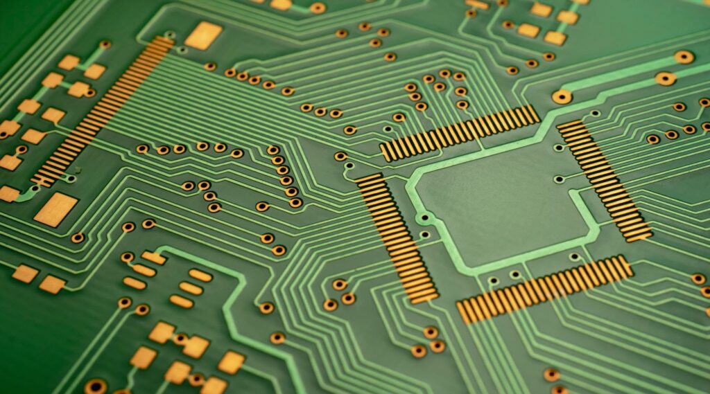
Once the circuit layout is finalized, the PCB manufacturing process can begin. The circuit layout is printed on a copper-clad board using a process called etching. The board is coated with a layer of photoresist, which is then exposed to UV light through a stencil of the circuit layout. The unexposed areas of the photoresist are then dissolved, leaving behind a pattern of copper on the board. This pattern of copper traces makes up the circuit.

Dragon Etching: Inside Look at PCB Manufacturing,test, from Workshop to Shipping | Sunset Delivery
PCB etching machine plants

PCB Etching:

Etching is the process of removing unwanted copper from the PCB to create the desired circuit pattern. It is done by exposing the board to an etchant, which selectively removes the copper from the areas not protected by the photoresist. After the etching process is complete, the remaining photoresist is stripped away, leaving behind the desired circuit pattern.

Home
PCB Etching Machine

PCB Developing Exposing:

The board is then developed using a chemical solution that dissolves the exposed photoresist, leaving behind the copper pattern that makes up the circuit. This process is known as developing.

Home
PCB Developing Exposing Machine

PCB Stripping:

Once the copper pattern is developed, the remaining photoresist must be stripped away using a chemical solution, leaving only the copper traces behind. This process is known as stripping.

Home
PCB Stripping Machine

PCB Cleaning:

After stripping, the board is thoroughly cleaned to remove any chemical residue and ensure a clean surface for the next step.

Home
PCB Cleaning Machine

PCB Desoldering:

During the assembly process, electronic components may need to be removed or replaced, requiring desoldering. This is done using specialized tools and techniques to remove the solder holding the component in place without damaging the board or the component.

Home
PCB Desoldering Machine

PCB Oxidation Resistance:

PCBs are susceptible to oxidation, which can cause corrosion and damage to the board over time. To prevent this, a layer of oxidation-resistant material is applied to the board to protect it from the environment.

Home
PCB Oxidation Resistance Machine

PCB Polishing:

Home
PCB Polishing Machine

After the oxidation-resistant layer is applied, the board may be polished to create a smooth surface and ensure the proper thickness of the copper traces.

PCB Sandblasting:

In some cases, the board may be sandblasted to create a rough surface for improved adhesion of the oxidation-resistant material.

Home
PCB Sandblasting Machine

PCB Browning:

Finally, the board may be treated with a chemical solution to create a brown or black surface that provides a contrast for easier inspection and testing.

In conclusion, the production of PCBs involves a series of steps that require precision, expertise, and specialized equipment. The PCB production process is critical to the functioning and performance of electronic devices, and it must be executed with care and attention to detail.

Home
PCB Browning Machine