Chemical etching remains one of the most versatile and cost‑effective methods for producing intricate steel components. This guide is tailored for material scientists and process engineers, presenting best practices—from alloy selection to post‑etch treatments—and highlighting case studies from industry leaders.
1. Steel Alloy Selection for Optimal Etching
Choosing the right steel alloy is critical to achieving uniform etch depth and pattern fidelity. Below is a comparative overview of common steels and their reactivity with two popular etchants:
Steel Type
Composition Highlights
Reactivity with Nitric Acid
Reactivity with Ferric Chloride
Typical Applications
Carbon Steel
Fe + 0.05–0.30% C
Moderate; risks surface passivation
High; fast material removal
Decorative panels, industrial brackets
Stainless Steel (300‑Series)
Fe + 16–18% Cr, 8–10% Ni
Low; strong passive film
Moderate; requires activation
Food equipment, medical instruments
Stainless Steel (400‑Series)
Fe + 11–17% Cr, <1% Ni
Moderate; breaks Cr₂O₃ layer
High; aggressive attack
Cutlery, aerospace components
Tool Steel
Fe + 0.5–1.5% C, W/Mo/Cr additives
Variable; dependent on alloy
Low–Moderate; slower etch rate
Precision dies, cutting tools
Table 1: Reactivity comparison for steel alloys with common etchants.
2. Chemical Etchant Formulations & Safety Protocols
Formulation of the etchant bath not only dictates etch rate and surface finish but also determines the necessary safety measures.
Acidic Baths
Nitric Acid (HNO₃): Typical concentration of 10–20% v/v in water. Provides smooth finishes but can over‑passivate stainless grades.
Ferric Chloride (FeCl₃): Often used at 15–25% w/v, especially for carbon and 400‑series stainless steels.
Alkaline Baths
Sodium Hydroxide (NaOH) with added wetting agents can be used for selective degreasing and mild etching of tool steels.
Safety Protocols:
Always don acid‑resistant gloves, face shield, and apron when handling corrosive baths.
Maintain local exhaust ventilation to capture harmful NO₂ or Cl₂ vapors.
Neutralize spent baths to pH 7–8 before disposal to comply with OSHA Chemical Hazards and EPA regulations.
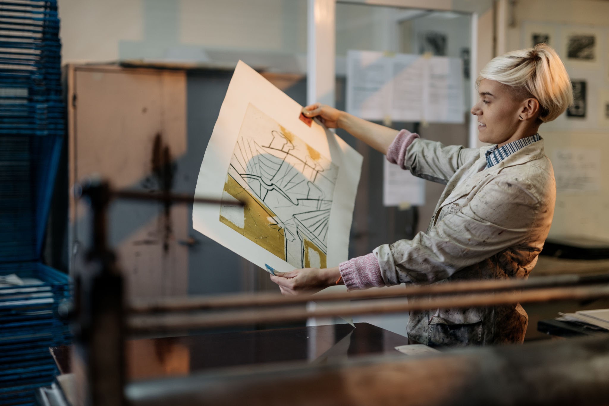
3. Masking Techniques for High‑Resolution Patterns
Achieving sub‑0.1 mm features demands precise masking:
Laser‑Cut Stencils
Best for durable, reusable patterns on thicker substrates (>0.5 mm).
Case Study: Microdrop Technologies Case Studies describes how they used laser stencils to etch shim stock for aerospace gauges, reducing cycle time by 20%.
Photoresist Films
Ideal for ultra‑fine features on thin steel foils.
DuPont Riston® photoresist offers excellent adhesion and resolution down to 25 µm; see DuPont Riston® Photoresist.
Tip: Always perform a contact angle test to verify photoresist wetting before exposure.
4. Temperature & Agitation Control for Consistency
Maintaining uniform temperature and controlled agitation is vital to prevent undercutting and edge thinning, especially for thin sheets:
Real‑Time Monitoring:
Inline thermocouples with ±0.5 °C accuracy keep bath temperature within 0.5 °C of setpoint.
Agitation Methods:
Mechanical Stirring: Provides robust mixing but can introduce turbulence.
Ultrasonic Agitation: Offers gentle, cavitation‑enhanced etching—ideal for delicate geometries.
Modern Machine Shop reports that switching from mechanical to ultrasonic agitation cut etch‑time variance by 30% in their pilot runs; see their article on Ultrasonic Etching Benefits.
5. Post‑Etch Treatments: Passivation & Coating
After etching, surface integrity and corrosion resistance must be restored or enhanced:
Passivation
Stainless Steels: Treat with a nitric acid bath per ASTM A967 Standard guidelines to remove embedded iron and regenerate the Cr₂O₃ layer.
Coating Options
Black Oxide: A low-build finish for corrosion resistance and reduced light reflection—commonly applied via hot alkaline baths. For details, see the All Metals Processing Black Oxide Guide.
Electroplating: Nickel or zinc plating for decorative and protective layers; ensure thorough rinsing to avoid under‑film corrosion.
Mastering steel chemical etching involves an interplay of alloy chemistry, etchant formulation, masking precision, and process control—capped by robust post‑etch treatments. By following these guidelines and leveraging industry‑proven techniques, metallurgists and engineers can achieve consistent, high‑resolution results tailored to their application’s demands.
Photo etching is proving to be an essential technology in aerospace manufacturing by addressing the high demands of precision, durability, and regulatory compliance. From etching titanium for lightweight structural components to developing ceramic-loaded masking for high-temperature alloys, the process has been refined to meet the extreme standards required in aerospace applications.
With robust non-destructive testing methods ensuring component integrity, adherence to AMS 2701 surface finish requirements, and exciting new integrations with additive manufacturing hybrids, photo etching is setting new benchmarks in aerospace production. This advanced process not only enables the creation of high-performance components but also supports the relentless pursuit of safety, efficiency, and innovation in the aerospace industry.
By embracing these technologies, aerospace engineers and QA specialists are empowered to push the envelope of design and performance—ensuring that every component meets the demanding operational standards of modern aviation and space exploration.
Titanium Etching for Lightweight Structural Components
Titanium is renowned for its excellent strength-to-weight ratio, making it indispensable in aerospace structures. However, etching titanium presents unique challenges:
Heat Resistance: The etching process must maintain titanium’s integrity under extreme operating temperatures without compromising its mechanical properties.
Stress Corrosion Cracking Mitigation: Special attention is required to prevent stress corrosion cracking during the etching process. This involves optimized etchant chemistries and carefully controlled process parameters to minimize residual stresses.
Advanced techniques in photo etching now enable the precise removal of material from titanium components, contributing to significant weight reductions while preserving structural strength and durability. This approach is instrumental in developing next-generation lightweight aerospace structures.
Masking Techniques for High-Temperature Alloys
High-temperature alloys, such as Inconel used in turbine blades, present additional complexities in etching due to their robust mechanical and thermal properties. Overcoming these challenges requires the use of innovative masking techniques:
Ceramic-Loaded Resists: Incorporating ceramic particles into photoresist materials enhances their thermal stability, making them ideal for etching Inconel turbine blades. The ceramic-loaded resist ensures that the mask remains intact even under high-temperature exposure, preserving critical areas from unwanted etching.
These advanced masking techniques allow for the precise definition of intricate geometries on high-temperature alloys, ensuring that components can withstand extreme operational conditions in turbine environments.
Non-Destructive Testing (NDT) Post-Etch
Ensuring the integrity of aerospace components after photo etching is paramount. Non-destructive testing (NDT) methods are employed to verify that the etching process has not introduced structural defects:
Eddy Current Testing: This technique is particularly effective at detecting micro-cracks in critical components such as fuel nozzles. Eddy current testing provides a rapid, reliable means of assessing surface integrity without impairing component performance. By meticulously scanning etched surfaces, engineers can ensure that any potential defects are identified and rectified before the components are deployed.
The integration of NDT into the post-etch process reinforces quality assurance and reliability standards critical for aerospace applications.
AMS 2701 Compliance: Surface Finish Requirements
For aerodynamic efficiency and performance, surface finish is a critical parameter in aerospace components. The AMS 2701 standard specifies rigorous surface finish requirements:
Achieving Ra <0.8μm: For components exposed to aerodynamic forces, such as skin panels or sensor housings, attaining a surface roughness below Ra <0.8μm is essential. Photo etching has evolved to meet this requirement through advanced process control, ensuring that etched surfaces are both smooth and precise.
The following table summarizes the surface finish requirements and how photo etching meets these criteria:
Requirement
Conventional Methods
Photo Etching
Surface Roughness (Ra)
Often exceeds 0.8μm
Achieves precise <0.8μm finishes
Consistency
Variable due to mechanical processes
Highly reproducible due to controlled chemical reactions
Meeting these stringent surface standards is imperative for ensuring the aerodynamic efficiency and longevity of aerospace components.
Future Frontiers: Etching in Additive Manufacturing Hybrids
The convergence of photo etching and additive manufacturing (AM) represents a significant leap forward in aerospace engineering innovation. This hybrid approach opens new avenues in component design and performance enhancement:
Integrated Etched Cooling Channels: One groundbreaking application is the integration of etched cooling channels into 3D-printed rocket engine components. By etching precisely defined channels into additively manufactured parts, engineers can enhance thermal management capabilities, crucial for maintaining engine performance under extreme conditions.
Design Flexibility: Hybrid processes enable complex geometries that are unattainable with conventional manufacturing, paving the way for advanced engine designs.
This visionary integration of photo etching with additive manufacturing is driving the next wave of aerospace innovation, combining the best of both technologies for superior performance and efficiency.
For further insights on the future of hybrid manufacturing techniques in aerospace, resources from NASA and SAE International provide ongoing research and expert analysis.
Innovative advances in photo etching are paving the way for a more sustainable manufacturing future. From closed-loop recycling systems that minimize chemical waste to the transition from mercury vapor lamps to energy-efficient LED units, eco-friendly photo etching technologies offer numerous benefits for both the environment and production efficiency.
The exploration of biodegradable photoresists further underscores the industry’s commitment to sustainability, while zero-discharge facilities serve as powerful proof points for what is possible with innovative water and chemical management solutions. Compliance with REACH and RoHS ensures that these advancements meet global standards, making them attractive not only from an environmental standpoint but also from a regulatory perspective.
Embracing these sustainable manufacturing practices can dramatically reduce the environmental footprint of photo etching, helping organizations achieve their green objectives and set new industry benchmarks for eco-friendly production. For ongoing updates and best practices in sustainable manufacturing, resources from EPA and the European Chemicals Agency are invaluable tools for further exploration.
Reducing Chemical Waste with Closed-Loop Systems
A major environmental challenge in photo etching is the management of chemical waste. Traditional systems often result in excessive disposal of etchants, which can be harmful to the environment. Recent breakthroughs in closed-loop systems are dramatically changing this scenario:
Etchant Recycling Technologies: Cutting-edge methods now allow for the regeneration of copper chloride and other etchants. By continuously recycling these chemicals, manufacturers can reduce waste and lower operating costs, while also adhering to environmental best practices.
Regulatory compliance with environmental standards such as REACH and RoHS.
For further reading on sustainable chemical recycling, the Environmental Protection Agency offers detailed insights into industry best practices.
Energy Efficiency in UV Exposure Units
Energy consumption is a critical concern in manufacturing. Advances in UV exposure units have shifted the balance toward more sustainable practices through innovative lighting solutions.
LED vs. Mercury Vapor Lamps: The transition from mercury vapor lamps to LED UV exposure units has resulted in a dramatic 40% reduction in energy consumption. This shift not only lowers energy bills but also minimizes harmful emissions associated with mercury use.
Below is a comparative table highlighting key differences:
Lighting Technology
Energy Consumption
Environmental Impact
Mercury Vapor Lamps
Higher energy usage
Potential mercury hazards
LED UV Exposure Units
40% lower energy consumption
Lower emissions and safer disposal
Table: Comparison of energy efficiency and environmental impact between traditional mercury vapor lamps and modern LED UV exposure units.
This transition is critical for manufacturers seeking to reduce their environmental footprint, aligning with global sustainability goals.
Biodegradable Photoresists: Fact or Fiction?
The materials used in photo etching are also under scrutiny for their environmental impact. One area of emerging interest is the development of biodegradable photoresists.
Soy-Based Resists: Researchers and industry pioneers are exploring soy-based resists as a renewable alternative to conventional photoresists. Preliminary studies suggest that these resists can deliver comparable performance while being significantly more eco-friendly.
Compostable Masking Films: Similarly, compostable masking films are being developed to replace traditional non-degradable materials. Although still in the nascent stages of market adoption, these innovations promise a reduction in landfill waste and a more sustainable lifecycle for etching processes.
These developments are exciting, yet they prompt the question: Are biodegradable photoresists a viable long-term solution? Continuous research and pilot programs are essential to confirm their effectiveness and scalability.
Case Study: Zero-Discharge Etching Facilities
Innovative implementations of sustainable photo etching are already making a tangible impact. A notable case study involves a German supplier who established a zero-discharge etching facility. Here are the key achievements of the facility:
95% Water Reuse: By integrating advanced water treatment and recycling systems, the facility achieved an impressive 95% water reuse rate. This not only drastically cuts water consumption but also minimizes the environmental impact of the etching process.
Zero Chemical Discharge: The closed-loop operation effectively eliminates the discharge of hazardous chemicals, ensuring compliance with strict environmental regulations and setting a benchmark for sustainable manufacturing.
For more details on pioneering sustainable manufacturing practices in Europe, the European Chemicals Agency is an excellent resource.
Certifications & Compliance (REACH, RoHS)
Adhering to environmental regulations is critical for companies operating in global markets. The integration of sustainable practices in photo etching must align with key certifications and regulations:
REACH Compliance: Manufacturers must ensure that all chemical substances used in the photo etching process comply with the European Union’s REACH regulation, which aims to protect human health and the environment from the risks posed by chemicals.
RoHS Certification: The Restriction of Hazardous Substances (RoHS) directive further mandates limitations on specific hazardous materials. Meeting these standards is crucial for suppliers operating in defense, medical, and consumer electronics sectors.
Navigating Global Supply Chains: A comprehensive understanding of these certifications ensures that sustainable manufacturing practices are not only environmentally beneficial but also commercially viable. Suppliers that meet these standards gain a competitive edge in global markets.
Environmental officers and sustainability advocates should closely monitor these regulations to drive continuous improvements in eco-friendly manufacturing technologies.
Proper maintenance is essential for ensuring consistent performance and longevity of PCB etching equipment. Without a structured upkeep plan, nozzle clogging, chemical imbalances, and pump failures can lead to downtime and costly repairs. This guide provides a comprehensive checklist to help PCB facility managers and technicians keep their equipment in optimal condition.
1. Daily/Weekly Maintenance Routines for Spray Etchers
Routine maintenance ensures uniform etching results and prevents unexpected failures. Below is a breakdown of daily and weekly tasks:
Task
Frequency
Why It’s Important?
Clean nozzles
Daily
Prevents clogging and ensures even etchant distribution.
Check pH and chemical concentration
Daily
Maintains optimal etching conditions for consistent results.
Inspect conveyor belts
Weekly
Reduces misalignment issues that can cause uneven etching.
Flush etchant system
Weekly
Prevents sediment buildup that can affect etch rates.
Best Practice: Using ultrasonic cleaning for nozzles can significantly improve etching uniformity by preventing micro-blockages.
2. Preventing Corrosion in Machine Components
Etching chemicals are highly corrosive, leading to machine wear and failure over time. Choosing the right materials and applying protective coatings can prevent damage.
Material Choices for Corrosion Resistance:
Component
Best Material Choice
Why?
Nozzles & Spray Bars
Titanium
Resistant to strong etchants like ferric chloride.
Tanks & Piping
Stainless Steel 316L
High resistance to chemical degradation.
Bearings & Conveyor Parts
PTFE-Coated Alloys
Prevents metal degradation from prolonged chemical exposure.
Industry Insight:Mitsubishi PCB Equipment uses titanium nozzles in their high-end etchers, reducing maintenance costs by 30% over five years. Source
3. Scheduled Downtime for Pump and Filter Overhauls
Regular pump and filter maintenance prevents clogging, pressure drops, and uneven etching.
Step-by-Step Guide for Pump & Filter Maintenance:
✅ Turn off the etching machine and drain etchant tanks. ✅ Inspect and replace worn pump diaphragms (typically every 3-6 months). ✅ Check for clogged filters and clean/replace them as needed. ✅ Refill system and test pump pressure before resuming production.
Maintenance Task
Frequency
Warning Signs
Replace pump diaphragms
Every 3-6 months
Reduced etchant flow, inconsistent spray pattern
Clean filter screens
Monthly
Visible sediment buildup, pressure fluctuations
Check spray pressure calibration
Quarterly
Uneven etching, excessive undercutting
Pro Tip: Keep spare filters and diaphragms in stock to reduce downtime during maintenance cycles.
4. Software Updates and Firmware Patches
Modern etching machines use firmware and software for process control, error logging, and predictive maintenance. Keeping these systems updated ensures optimal performance and prevents security vulnerabilities.
Why Software Updates Matter:
🛠 Fixes bugs that may cause erratic machine behavior.
📊 Enhances process monitoring for real-time fault detection.
🔄 Improves compatibility with new automation features.
Update Type
Why It’s Needed?
How Often?
Firmware Patches
Improves machine logic and error handling
Every 6-12 months
Software UI Updates
Enhances operator experience, adds new features
Annually
Security Patches
Prevents hacking risks in networked systems
As released
Case Study: A leading PCB manufacturer reduced unexpected downtime by 40% after implementing automatic firmware updates on their LPKF etching machines. Source
5. Emergency Protocols: Handling Chemical Spills and Power Failures
Unexpected failures like chemical spills or power outages can be hazardous. Having emergency response protocols in place protects workers, equipment, and production schedules.
Chemical Spill Response Checklist
🧯 Use OSHA-compliant spill kits for rapid containment. 🛑 Shut down affected equipment to prevent further contamination. 🧼 Neutralize spills with appropriate agents (e.g., sodium bicarbonate for acid spills). 📢 Report and document the incident per facility guidelines.
Power Failure Backup Plan
🔋 Install an Uninterruptible Power Supply (UPS) to protect critical systems.
⚡ Use backup generators for prolonged outages.
🖥 Enable automatic data logging to resume processes smoothly after a restart.
Best Practice: Implement yearly emergency drills to ensure all staff are familiar with chemical spill and power failure protocols.
Final Thoughts
By following a structured maintenance schedule, PCB facility managers and technicians can significantly extend the lifespan of etching machines, reduce downtime, and improve etching consistency.
✅ Daily & weekly routines keep the machine running efficiently. ✅ Corrosion prevention saves money on part replacements. ✅ Scheduled downtime for pumps & filters prevents sudden failures. ✅ Software updates enhance performance & security. ✅ Emergency protocols protect workers and maintain compliance.
Would you like me to provide a printable maintenance checklist template? 🚀
Selecting a PCB etching machine is a critical decision that impacts production efficiency, cost-effectiveness, and long-term scalability. For non-technical teams like PCB product managers and procurement specialists, understanding key specifications without deep technical expertise can be challenging. This guide simplifies the process, helping you make an informed purchase.
1. Key Specs to Compare: Throughput, Board Size, and Automation
Throughput: Measured in panels per hour, this determines production efficiency.
Board Size Compatibility: Ensures the machine can handle your required maximum panel dimensions.
Automation Level: Impacts labor requirements and process consistency.
Wet Film Precision Metal Etching Process
Specification
Why It Matters
Typical Ranges
Throughput (Panels/Hour)
Higher throughput = faster production
20 – 200 panels/hour
Max Board Size
Must match your largest PCB design
18” × 24” to 24” × 36”
Automation Level
Reduces operator dependency
Manual, Semi-automatic, Fully Automated
Industry Example:LPKF offers high-precision etching solutions with fully automated process control, ensuring minimal operator intervention and high yield. Source
2. Cost Analysis: Upfront Investment vs. Long-Term ROI
Beyond the purchase price, consider hidden costs that affect the total cost of ownership (TCO).
Cost Breakdown
Cost Factor
Upfront or Ongoing?
What to Consider?
Machine Price
Upfront
High-end models offer automation, but at a cost.
Chemical Disposal
Ongoing
Safe disposal regulations increase expenses.
Maintenance & Repairs
Ongoing
Higher for complex or proprietary systems.
Energy Consumption
Ongoing
High-powered etching systems use more electricity.
Pro Tip: Some vendors offer modular upgrades, allowing you to start with a basic model and scale up as needed—reducing initial costs.
3. Vendor Evaluation: Service Contracts and Technical Support
Choosing the right vendor is as important as selecting the right machine. Look beyond the product and evaluate:
Warranty terms – What parts/labor are covered?
Service contracts – Do they offer on-site support or just remote assistance?
Spare parts availability – Can replacements be sourced easily?
Red Flags to Watch Out For:
❌ Short warranty periods (<1 year) ❌ Limited service locations ❌ Expensive proprietary parts
Case Study:Mitsubishi PCB Equipment provides extensive global support, reducing downtime for large-scale manufacturers. Source
4. Future-Proofing: Scalability for Advanced PCB Materials
With the rise of flexible circuits, RF boards, and HDI designs, selecting a machine that can handle next-gen PCB materials is crucial.
Material Type
Etching Challenges
Best Machine Features
FR4 (Standard PCBs)
Standard etching process
Any high-precision etcher
Flexible PCBs
Requires low-stress etching
Fine spray nozzles, low-pressure settings
High-Frequency (Rogers, PTFE)
Sensitive to chemical variations
Temperature-controlled etchant baths
Recommendation: If you’re producing RF or flexible PCBs, ensure your etching machine is compatible with non-standard substrates to avoid expensive upgrades later.
5. Real-World User Reviews: What Manufacturers Wish They Knew
Many buyers realize post-purchase that certain machine limitations could have been avoided. Below are insights from PCB manufacturers:
💬 “We didn’t account for the cost of chemical disposal, and it’s adding up fast.” 💬 “Our vendor’s support team is slow—downtime kills our production schedule.” 💬 “We should have gone for a model with automation; manual tuning is a nightmare.”
Top-Rated Brands Based on User Feedback:
⭐ LPKF – Best for precision etching and automation ⭐ Mitsubishi – Reliable, high-throughput production ⭐ EtchMaster – Cost-effective for small/mid-scale production
Final Thoughts
For non-technical teams, the best approach to choosing a PCB etching machine is to balance:
✅ Technical capability – Matches your production requirements ✅ Total cost – Includes hidden expenses, not just the purchase price ✅ Vendor reliability – Strong support and service contracts
By considering these factors, you can make a strategic investment that ensures high efficiency, lower costs, and future scalability.
Need help evaluating specific models? Let me know your production needs, and I’ll suggest the best options! 🚀
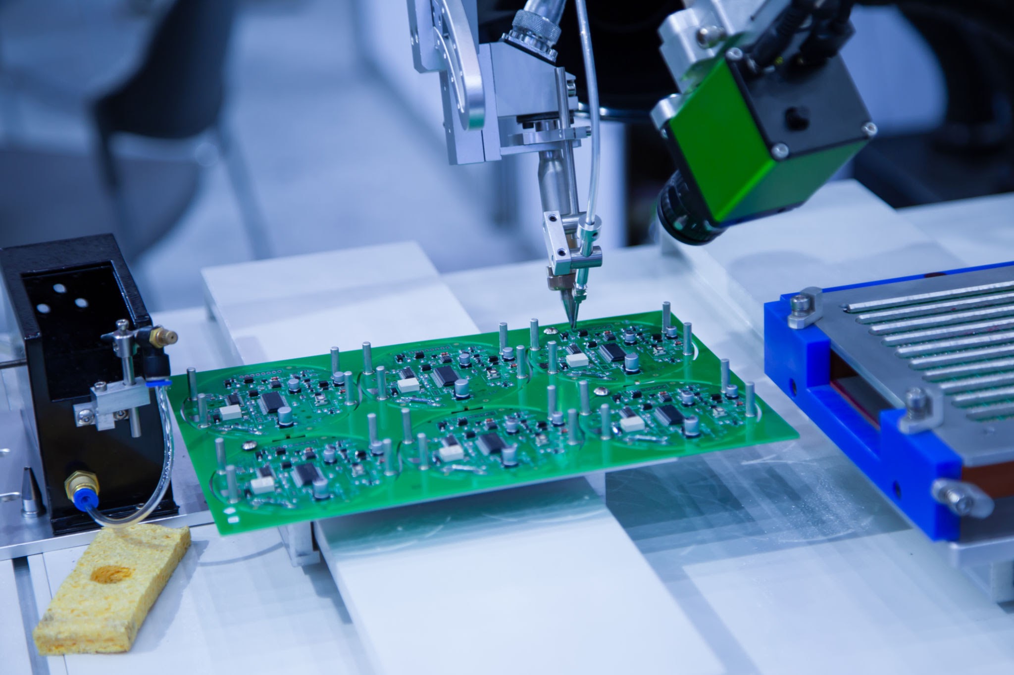
Printed Circuit Board (PCB) etching is a critical step in manufacturing, determining the precision and quality of the final product. To achieve high-yield production, optimizing etching machine parameters is essential. This guide explores key parameters that influence etch rate, resolution, and defect reduction.
Understanding Etching Rate vs. Resolution Trade-offs
The relationship between etch rate and resolution directly impacts trace width precision and undercutting. Higher etch rates can speed up production but may lead to excessive undercut, affecting circuit integrity.
Etching Factor
Impact on Resolution
Recommended Action
Etchant Strength
High strength speeds etching but risks over-etching
Maintain optimal chemical balance
Etching Time
Shorter time minimizes undercut but requires strong control
Fine-tune based on material thickness
Board Material
Different materials react at varying speeds
Adjust process based on material properties
Industry Insight: According to PCBWay, etching speed should be carefully balanced to avoid signal integrity issues in high-density interconnect (HDI) PCBs.
Temperature and Chemical Concentration Calibration
Maintaining the correct etchant temperature and chemical concentration ensures uniform etching results. The two most common etchants are ferric chloride (FeCl₃) and ammonium persulfate (NH₄)₂S₂O₈), each with distinct behaviors.
Ferric Chloride (FeCl₃): High etching power, but prone to sludge formation.
Ammonium Persulfate (NH₄)₂S₂O₈): Provides smoother etching but requires precise temperature control.
Parameter
Ferric Chloride
Ammonium Persulfate
Optimal Temperature
40-50°C
50-60°C
Etch Rate Control
Moderate
More Sensitive
Common Issues
Residue Formation
Requires frequent concentration monitoring
Best Practice: Regularly measure etchant concentration and refresh the solution to maintain efficiency.
Nozzle Pressure Optimization for Uniform Etching
Spray etching machines use nozzle pressure to evenly distribute etchant, ensuring precise material removal. Pressure calibration is crucial for multilayer boards.
Key Considerations for Nozzle Optimization:
Low pressure leads to uneven etching and defects.
High pressure risks over-etching and material weakening.
Optimal pressure ensures consistent removal rates and sharp trace edges.
Nozzle Pressure
Impact on PCB
Too Low
Incomplete etching, residual copper
Too High
Excessive material loss, reduced yield
Optimized
Uniform traces, minimal defects
Industry Example:AT&S, a leading PCB manufacturer, utilizes precision nozzle pressure control systems to achieve high-density PCB manufacturing with minimal defects.
Automated vs. Manual Parameter Adjustments
Modern closed-loop automation systems dynamically adjust etching parameters in real time, while traditional manual tuning relies on operator expertise.
Method
Advantages
Challenges
Manual Tuning
Lower initial cost, flexibility
Inconsistent quality, operator-dependent
Automated System
Consistent etching, real-time adjustments
Higher setup cost, requires software integration
Case Study: A comparison by Camteksource shows that automated etching systems improve process stability, especially in fine-pitch PCBs.
Optimizing PCB etching machine parameters requires a fine balance between etch rate, resolution, and process automation. Leveraging automated controls, calibrated chemical solutions, and optimized nozzle pressure ensures high-yield production with minimal defects.
The increasing concern over environmental sustainability has prompted industries across the globe to explore greener alternatives for manufacturing. In the world of wearable and flexible electronics, thin film heaters are no exception. With the demand for more sustainable products, there is a growing interest in developing eco-friendly thin film heaters that not only reduce e-waste but also contribute to a circular economy. This article explores the latest advancements in eco-friendly materials and manufacturing processes, including recyclable substrates, energy-efficient production techniques, and innovations in reducing emissions during the production of thin film heaters.
Recyclable and Biodegradable Substrates: Reducing E-Waste
A major challenge in the manufacturing of electronic devices is the accumulation of electronic waste, or e-waste. Many traditional heating elements use materials that are difficult to recycle, contributing significantly to environmental pollution. However, recent developments in sustainable substrates are offering promising solutions.
One of the most exciting innovations is the use of cellulose nanofiber films as a substrate material for thin film heaters. These biodegradable films are derived from plant-based sources, offering a renewable and recyclable alternative to conventional materials. By replacing petroleum-based substrates with cellulose-based ones, manufacturers can significantly reduce the environmental impact of their products, especially at the end of their lifecycle.
Key Benefits of Cellulose Nanofiber Films:
Biodegradable: Breaks down naturally, reducing landfill impact.
Renewable: Sourced from sustainably harvested plant materials.
High Strength: Exhibits similar mechanical properties to synthetic polymers.
Lifecycle Assessment: Roll-to-Roll Production vs. Traditional Wire-Based Heaters
When evaluating the sustainability of thin film heaters, it is essential to consider the entire lifecycle of the product, including manufacturing and disposal. Traditional wire-based heaters require the use of metallic wires that must be individually fabricated and connected, which is both labor and energy-intensive. In contrast, the roll-to-roll production process used for thin film heaters offers several environmental advantages.
Roll-to-roll production is a continuous process that can be highly energy-efficient, reducing energy consumption compared to traditional methods. Additionally, the process generates less waste and uses fewer materials. In a lifecycle assessment, roll-to-roll production has been shown to deliver significant energy savings over the long term, helping to lower the carbon footprint of the product.
Benefits of Roll-to-Roll Production:
Energy Efficiency: Consumes less energy than traditional wire-based methods.
Waste Reduction: Minimal material wastage due to the continuous nature of the process.
Scalability: Suitable for mass production while maintaining sustainability.
Solvent-Free Deposition Techniques: Reducing VOC Emissions by 70%
The manufacturing process of thin film heaters typically involves the use of solvents in deposition techniques, such as in the creation of conductive coatings. These solvents often release volatile organic compounds (VOCs), which contribute to air pollution and can be harmful to human health. To address this, manufacturers are increasingly turning to solvent-free deposition techniques.
Recent advancements in solvent-free processes, such as dry deposition or aerosol jet printing, have shown great promise in reducing VOC emissions by up to 70%. By eliminating the need for harmful solvents, these techniques help minimize the environmental impact of production while maintaining high performance and durability in the finished product.
Key Advantages of Solvent-Free Deposition:
Lower VOC Emissions: Contributes to cleaner air and a healthier work environment.
Reduced Environmental Impact: Helps meet stricter regulations on air quality.
High-Quality Films: Maintains performance standards without the use of solvents.
Market Trends: Growth of OEKO-TEX® Certified Heating Pads in EU/NA Consumer Markets
As consumers become more eco-conscious, there is an increasing demand for products that are both effective and environmentally friendly. In particular, the market for OEKO-TEX® certified heating pads is seeing rapid growth, especially in the EU and North American consumer markets. These certifications indicate that the products meet stringent safety and sustainability standards, including the use of non-toxic, environmentally friendly materials.
OEKO-TEX® certification ensures that the heating pads have been tested for harmful substances and are produced using processes that minimize environmental impact. This certification is becoming a significant selling point for consumers who are looking for products that align with their green values, contributing to the growing popularity of sustainable heating solutions.
Market Insights:
OEKO-TEX® Growth: The demand for certified heating pads is increasing in environmentally-conscious regions.
Consumer Preferences: More consumers are prioritizing sustainability when purchasing heating products.
Regulatory Support: Stricter regulations in the EU and NA are driving the adoption of green technologies.
Conclusion
As the world shifts toward a green economy, the manufacturing of thin film heaters must evolve to meet both environmental and performance standards. By embracing sustainable materials like cellulose nanofiber films, adopting energy-efficient production methods such as roll-to-roll manufacturing, and reducing emissions through solvent-free deposition techniques, the industry is paving the way for more eco-friendly solutions. The growth of OEKO-TEX® certified products in consumer markets further underscores the increasing demand for sustainable heating technologies. These advancements not only contribute to a healthier planet but also open up new opportunities for businesses to align with the values of environmentally conscious consumers.
For more information on sustainable manufacturing practices in electronics, visit OEKO-TEX® or explore the lifecycle benefits of roll-to-roll production at Roll-to-Roll Research.
The growing demand for wearable technology that combines comfort, efficiency, and performance has spurred the development of ultrathin heating elements. These elements, designed for applications like medical-grade heating pads and smart textiles, must meet several challenging requirements: they must be thin, flexible, and capable of maintaining high performance over extended periods of use. The choice of materials for these heating elements is critical for achieving the desired balance of conductivity, flexibility, and thermal stability, particularly under cyclic bending. In this article, we will explore some of the most promising materials for ultrathin heating elements, compare their key properties, and highlight a case study involving medical applications.
Material Innovations Enabling Sub-100µm Thin Film Heaters
To create heating elements that are both efficient and lightweight, materials with exceptional electrical conductivity and flexibility are essential. Traditional materials like copper or aluminum are not ideal due to their bulkiness and limited performance under bending. As such, more innovative materials have emerged, including:
Silver Nanowires: These nanowires offer excellent electrical conductivity and are flexible enough to withstand numerous bend cycles without significant degradation. They are particularly valuable in applications requiring both high performance and lightweight features.
Graphene: Known for its superior conductivity, graphene also excels in flexibility and thermal stability. Its high surface area and ability to conduct heat efficiently make it a popular choice for ultrathin heaters.
Carbon Nanotubes (CNTs): CNTs have an ideal combination of high conductivity and mechanical strength, making them perfect for bending-resistant heating elements. However, their cost can be a limiting factor in large-scale production.
Material Comparison Table
To better understand the trade-offs between these materials, let’s compare them in terms of key properties like conductivity, flexibility, and thermal stability.
Material
Conductivity (S/m)
Flexibility (bend cycles)
Thermal Stability (°C)
Cost (USD per g)
Silver Nanowires
10⁶
10,000+
-50 to 300
0.1 – 1
Graphene
10⁶
5,000+
-50 to 500
1 – 10
Carbon Nanotubes
10⁶
15,000+
-50 to 450
5 – 20
The table above clearly shows that while all three materials offer high conductivity and good flexibility, there are key differences in cost and thermal stability. Silver nanowires, for instance, are the most affordable option, but graphene and CNTs offer better thermal stability at higher temperatures, which could be essential in some medical or industrial applications.
Case Study: Integration with Polyimide Substrates for Medical-Grade Heating Pads
One of the most compelling uses of ultrathin heating elements is in the medical field. In particular, wearable heating pads designed to help alleviate pain from conditions like arthritis have become a critical application. These pads need to provide consistent heat over long periods while maintaining user comfort and safety. The combination of flexible substrates like polyimide and advanced materials like silver nanowires or CNTs has made this possible.
Polyimide is particularly well-suited for wearable medical heating pads due to its high thermal stability, flexibility, and biocompatibility. It can withstand temperatures ranging from -269°C to 400°C, making it ideal for use in a variety of heating applications. When combined with silver nanowires, the resulting heater can maintain a steady operating range of 40–120°C, perfect for arthritis therapy.
Integration Challenges
Despite the promising material properties, several challenges remain in integrating these materials into reliable products. For instance, the scalability of CNTs and graphene for mass production remains a hurdle, as these materials are still relatively expensive. Additionally, manufacturers need to ensure that the heating elements maintain consistent performance through thousands of bend cycles without compromising flexibility or efficiency.
A notable example comes from ThermoSoft International, a company specializing in medical-grade heating pads. They have successfully integrated ultrathin flexible heaters into their products, targeting therapeutic heat for arthritis patients. Their innovations include using polyimide substrates combined with silver nanowires to achieve a balance of performance and cost-effectiveness for widespread distribution. You can learn more about their work on their official website.
Trade-offs Between Material Cost, Scalability, and Performance
When selecting the right material for ultrathin heating elements, it’s crucial to weigh the trade-offs between cost, scalability, and performance. Silver nanowires, while affordable and scalable, might not offer the same level of thermal stability as graphene or CNTs, especially at high temperatures. On the other hand, graphene and CNTs can provide superior performance but come at a higher cost, which might limit their use in consumer-grade applications.
As the demand for wearable heating technologies continues to grow, companies must navigate these trade-offs carefully to develop products that meet both the technical specifications and budget constraints of their target markets. Ultimately, the choice of material will depend on the specific application and performance criteria, whether it’s for medical devices, sportswear, or smart textiles.
Engineering managers and procurement specialists face the complex challenge of balancing performance and manufacturing costs when overseeing multilayer PCB projects. As electronic devices grow in complexity, multilayer PCBs (MLBs) have become essential for integrating more components in smaller spaces, offering increased functionality without compromising performance. However, designing and manufacturing these boards comes with significant cost considerations, which demand a strategic approach to material selection, lead time reduction, and sustainability practices. This chapter provides a comprehensive guide for decision-makers, focusing on how to optimize multilayer PCB projects while ensuring cost-effectiveness and high-quality output.
Wet Film Precision Metal Etching Process
Material Selection: High-Tg Laminates vs. Standard FR-4 for Thermal Management
One of the first decisions in multilayer PCB design is material selection, which impacts both performance and cost. High-Tg laminates and standard FR-4 are two of the most commonly used materials for PCB construction, but they serve different purposes.
High-Tg Laminates for Thermal Management
High-Tg (glass transition temperature) laminates are ideal for applications where thermal management is a concern, such as in consumer electronics, automotive, and industrial equipment. These laminates can withstand higher temperatures and are more stable, making them suitable for multilayer designs that need to endure heat generated by densely packed components.
Pros: High-Tg laminates offer superior thermal performance, reduce the risk of warping or delamination, and are essential for devices with high operating temperatures.
Cons: They are more expensive than standard FR-4 and can increase the overall production cost of the PCB.
Standard FR-4 for Cost-Effective Designs
On the other hand, FR-4 is a widely used, cost-effective material for many general-purpose PCB applications. It is suitable for designs that don’t require the same level of thermal stability but still provide reliable performance for a variety of products.
Pros: FR-4 is widely available, easy to process, and relatively inexpensive, making it ideal for budget-conscious projects.
Cons: It has a lower glass transition temperature compared to high-Tg laminates, limiting its use in thermally demanding applications.
Material Selection Trade-Offs for Multilayer Designs
Decision-Making Tip: For high-performance applications (such as aerospace or high-frequency RF circuits), investing in high-Tg laminates may be necessary, despite the added cost. For standard consumer electronics, where thermal stress is less of an issue, FR-4 provides a cost-effective solution.
Lead Time Reduction: Streamlining Panelization and Partnering with Agile Suppliers
Reducing lead times is crucial for keeping costs low and improving time-to-market for multilayer PCB projects. Two key strategies for achieving this are panelization optimization and partnering with agile suppliers.
Panelization Optimization
Panelization refers to the process of organizing multiple PCB designs onto a single large panel for efficient manufacturing. For multilayer PCBs, optimizing the panelization process can significantly reduce production lead times by improving material utilization and reducing waste.
Best Practices: Ensuring optimal panel size and spacing reduces setup time and minimizes scrap. Advanced software tools can automate panelization, reducing manual intervention and errors.
Partnering with Agile Suppliers
Building strong relationships with agile suppliers is essential for reducing lead time. Suppliers with flexible production capabilities can quickly adapt to design changes, scale production, and respond to urgent deadlines.
Key Benefits: Agile suppliers offer faster turnaround times, ability to adjust production schedules, and can handle complex multilayer designs with greater flexibility.
Lead Time Reduction Strategy Summary
Strategy
Benefits
Best Use Cases
Panelization Optimization
Reduces material waste, improves manufacturing efficiency
High-volume production, cost-conscious designs
Agile Supplier Partnership
Faster turnaround, flexibility in scheduling, quick response to design changes
Decision-Making Tip: When working with tight timelines, it’s worth considering the trade-off between panel size optimization and partnering with agile suppliers for quick revisions and fast manufacturing.
Sustainability Metrics: Recycling Etchant Waste and Reducing Chemical Usage
As environmental concerns continue to rise, manufacturers are under increasing pressure to adopt sustainable practices. For multilayer PCB projects, this includes managing etchant waste and reducing the chemical usage throughout the production process.
Recycling Etchant Waste
Etching is a vital step in the PCB fabrication process, but it can generate large amounts of chemical waste. To reduce environmental impact and comply with increasingly strict regulations, companies can implement etchant recycling systems. These systems allow manufacturers to reuse etchant chemicals, significantly reducing the volume of waste generated.
Benefits: Reduced disposal costs, lower chemical consumption, and a smaller environmental footprint.
Considerations: The initial cost of installing recycling systems and ongoing maintenance.
Reducing Chemical Usage
Efficient chemical management involves using optimized etching solutions that require less chemical volume to achieve the same result. This can be achieved by using advanced etching machines that deliver more precise and consistent chemical application.
Benefits: Lower chemical costs, reduced environmental impact, and less waste production.
Considerations: Investment in new technology or modifications to existing equipment.
Install etchant recycling systems, monitor chemical levels regularly
Reduced Chemical Usage
Lowers chemical costs, reduces waste
Use precision etching technologies, optimize chemical formulations
Decision-Making Tip: Sustainability should be prioritized in industries such as consumer electronics and aerospace, where environmental regulations are stricter. Investing in etchant recycling systems and chemical reduction technologies can yield long-term cost savings and improve corporate reputation.
ROI Scenarios: When to Invest in 8-Layer Boards vs. Simplifying the Design
One of the most significant decisions in multilayer PCB design is determining whether to invest in complex designs, such as 8-layer boards, or simplify the design to reduce costs. This decision should be based on factors such as performance requirements, budget constraints, and production capacity.
8-Layer Boards for High-Demand Applications
An 8-layer PCB allows for more dense and complex circuit designs, which is particularly useful in aerospace, medical devices, and high-performance computing. However, 8-layer boards increase manufacturing costs due to the additional layers, processing time, and material requirements.
When to Choose 8-Layer Boards: Choose 8-layer boards when the design requires complex routing, high-speed signal transmission, or the integration of multiple components within a limited footprint (such as aerospace applications or advanced communication systems).
Simplified Designs for Consumer Electronics
In contrast, simplified designs (such as 4-layer boards) may be sufficient for consumer electronics like smartphones, wearables, or home appliances. These designs offer a good balance between cost-effectiveness and performance, especially when the goal is to meet price-sensitive market demands.
When to Simplify the Design: Simplify designs when the application does not require high-density interconnects, high-speed performance, or complex routing.
Cost Comparison: Consumer Electronics vs. Aerospace Applications
Application
Typical Layers
Cost Impact
Best Use Cases
Consumer Electronics
4-6 Layers
Lower cost, faster production
Smartphones, wearables, home electronics
Aerospace
8 Layers or more
Higher cost, more complex manufacturing
Satellites, avionics, military electronics
Decision-Making Tip: If performance is the priority (e.g., in aerospace), investing in 8-layer boards makes sense, despite the higher cost. For consumer electronics, a simpler design often provides a sufficient balance of cost and performance.
Conclusion
Balancing performance and manufacturing costs when etching multilayer PCBs is a multifaceted challenge that requires careful consideration of materials, production strategies, and sustainability metrics. By making strategic choices in material selection, lead time reduction, and ROI evaluation, engineering managers and procurement specialists can optimize their multilayer PCB projects, ensuring high-quality results without exceeding budget constraints.
Through partnerships with agile suppliers, investments in sustainability practices, and a focus on cost-effective design, organizations can achieve significant long-term savings and performance enhancements, making them better positioned in competitive markets like consumer electronics and aerospace.
Product managers should weigh the trade-offs between etchant types, ROI considerations, environmental compliance, and supplier trends when choosing the right etching solution for their manufacturing needs. FeCl₃, H₂O₂ + H₂SO₄, and CuCl₂ each offer distinct advantages, but CuCl₂‘s ability to be recycled through closed-loop systems presents a particularly strong case for reducing overall costs, especially for high-volume operations.
Comparative Table: FeCl₃ vs. H₂O₂+H₂SO₄ vs. CuCl₂
Choosing the right etchant involves balancing cost, etch rate, and waste treatment complexity. The table below compares FeCl₃, H₂O₂+H₂SO₄, and CuCl₂ on these key metrics:
Etchant
Cost
Etch Rate
Waste Treatment Difficulty
FeCl₃ (Ferric Chloride)
Low to Medium
Moderate (5-8 µm/min at 35°C)
Moderate (requires neutralization and recycling)
H₂O₂ + H₂SO₄ (Hydrogen Peroxide + Sulfuric Acid)
Medium to High
High (10-15 µm/min at 40°C)
High (requires careful handling of both acidic and oxidizing wastes)
CuCl₂ (Copper Chloride)
Medium
High (8-12 µm/min at 40°C)
Low (can be recycled using closed-loop systems)
This table highlights that while H₂O₂ + H₂SO₄ offers a faster etch rate, it also presents higher waste treatment challenges compared to FeCl₃. However, CuCl₂ offers recyclability and low waste treatment difficulty, which can lead to long-term savings.
ROI Calculation: Automated Spray System vs. Immersion Etching for High-Volume MEMS Production
In high-volume MEMS production, the choice between automated spray systems and immersion etching can significantly impact cost efficiency and output quality.
ROI Breakdown:
Automated Spray System:
Initial investment: High (equipment purchase and installation).
Operational costs: Medium (lower etchant consumption, faster etch rates).
Maintenance: Low (requires less manual intervention, minimal downtime).
Throughput: High (can etch multiple substrates simultaneously).
Long-term ROI: High (due to reduced chemical waste, increased throughput, and better consistency).
Immersion Etching:
Initial investment: Low (simpler equipment).
Operational costs: High (more etchant required, slower etch rates).
Maintenance: Medium (manual cleaning, higher chemical usage).
Throughput: Medium (slower compared to spray systems).
Long-term ROI: Medium (higher waste disposal costs and slower production rates).
By investing in automated spray systems, product managers can expect a higher ROI in high-volume MEMS production due to lower chemical consumption and higher throughput, despite the initial capital investment.
Ensuring environmental compliance is a critical aspect of etching operations, especially when dealing with hazardous chemicals. Below is a checklist to help product managers stay compliant with OSHA regulations and ANSI Z400.1 for acid mist suppression:
Acid Mist Control:
Use local exhaust ventilation (LEV) systems to capture acid mist at the source.
Ensure that all ventilation systems are regularly inspected and maintained to meet OSHA standards.
Personal Protective Equipment (PPE):
Provide workers with acid-resistant gloves, face shields, and protective clothing.
Implement respirators or other respiratory protection systems in areas with high acid mist concentrations.
Etchant Waste Handling:
Install neutralization tanks for safe disposal of etchant waste.
Ensure proper labeling and documentation of all waste containers, following ANSI Z400.1 guidelines for hazardous materials.
Monitoring:
Regularly measure air quality for acid mist levels to ensure compliance with OSHA permissible exposure limits (PELs).
This checklist can help prevent workplace hazards while ensuring compliance with environmental and safety regulations.
Supplier Spotlight: 2023 Pricing Trends for Copper Chloride Recyclers in Southeast Asia
As copper chloride (CuCl₂) continues to grow in popularity due to its closed-loop recyclability system, here are some 2023 pricing trends for CuCl₂ recyclers in Southeast Asia:
Copper Chloride Recovery System Pricing:
On average, recycling prices in Southeast Asia have remained steady at around $3–$5 per liter for CuCl₂ recovery services, depending on the volume and contract length.
Some suppliers, like Pacific Etching Solutions, offer volume-based discounts, which can reduce the overall cost by up to 15% for high-volume customers.
Recycling Infrastructure Investment:
Many companies are investing in in-house CuCl₂ recycling units to take advantage of reduced long-term costs. Initial setup costs for these systems range from $100,000 to $200,000 depending on the scale of operation.
By switching to closed-loop CuCl₂ systems, manufacturers can expect substantial savings in waste disposal costs, potentially cutting expenses by 60%.
Key Takeaway:
Switching to closed-loop CuCl₂ systems can cut disposal costs by 60%. This makes CuCl₂ a highly cost-effective choice for high-volume etching operations in the long term, offering both environmental benefits and cost savings.
This website uses cookies so that we can provide you with the best user experience possible. Cookie information is stored in your browser and performs functions such as recognising you when you return to our website and helping our team to understand which sections of the website you find most interesting and useful.
Strictly Necessary Cookies
Strictly Necessary Cookie should be enabled at all times so that we can save your preferences for cookie settings.
If you disable this cookie, we will not be able to save your preferences. This means that every time you visit this website you will need to enable or disable cookies again.