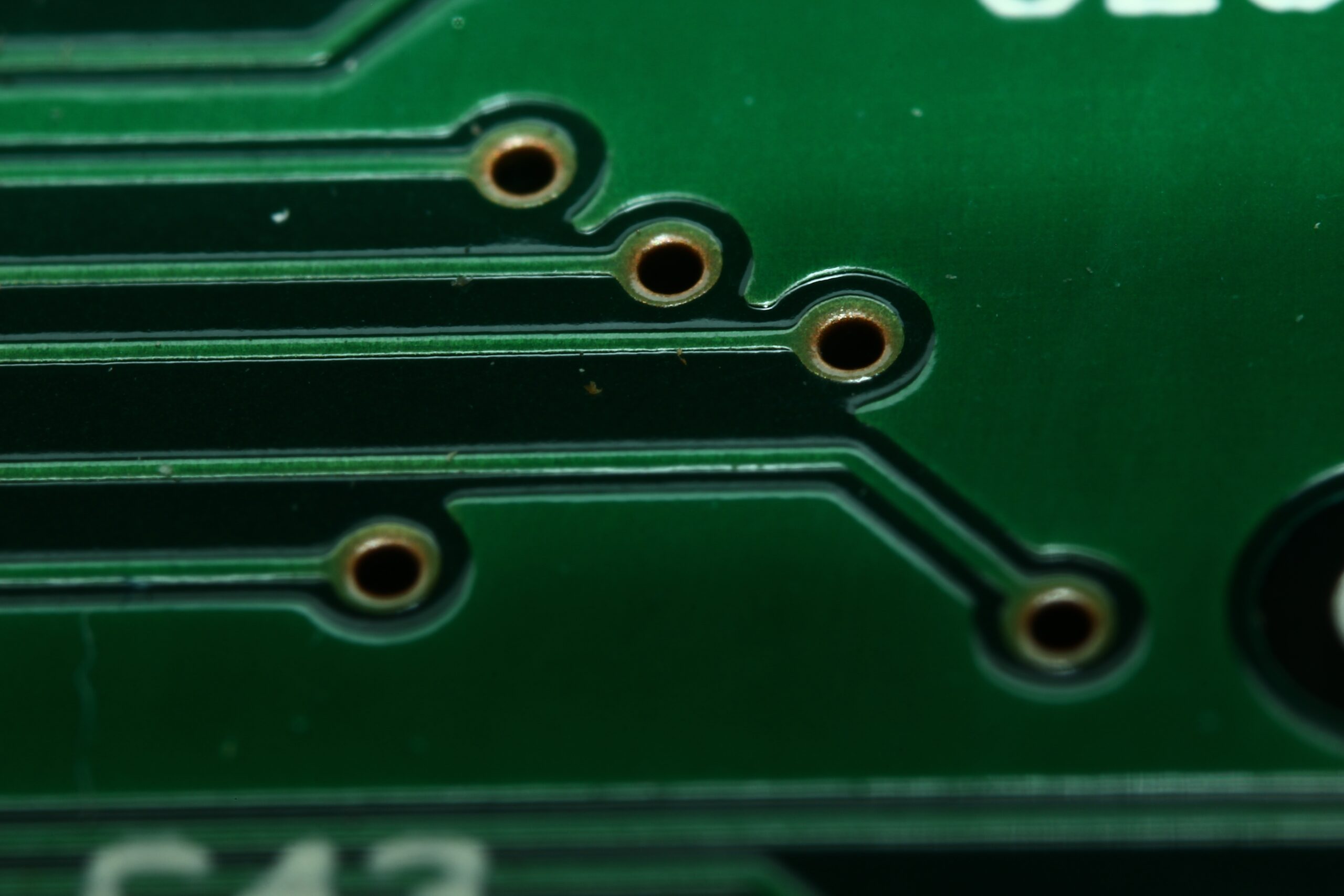
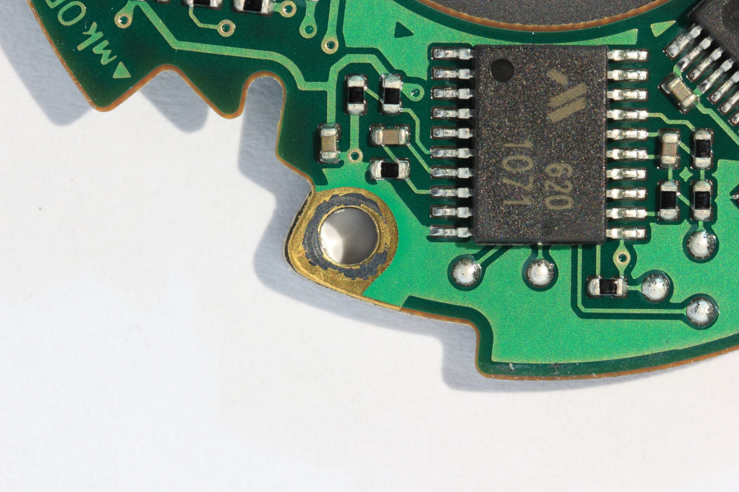
Tag Archives: PCB Manufacturing

Unveiling the Intricate Manufacturing Process of PCBs: Building the Backbone of Electronics

Discover the complex steps involved in creating printed circuit boards (PCBs) and their vital role in powering modern electronics.

The Intricate Manufacturing Process of PCBs: Building the Backbone of Modern Electronics

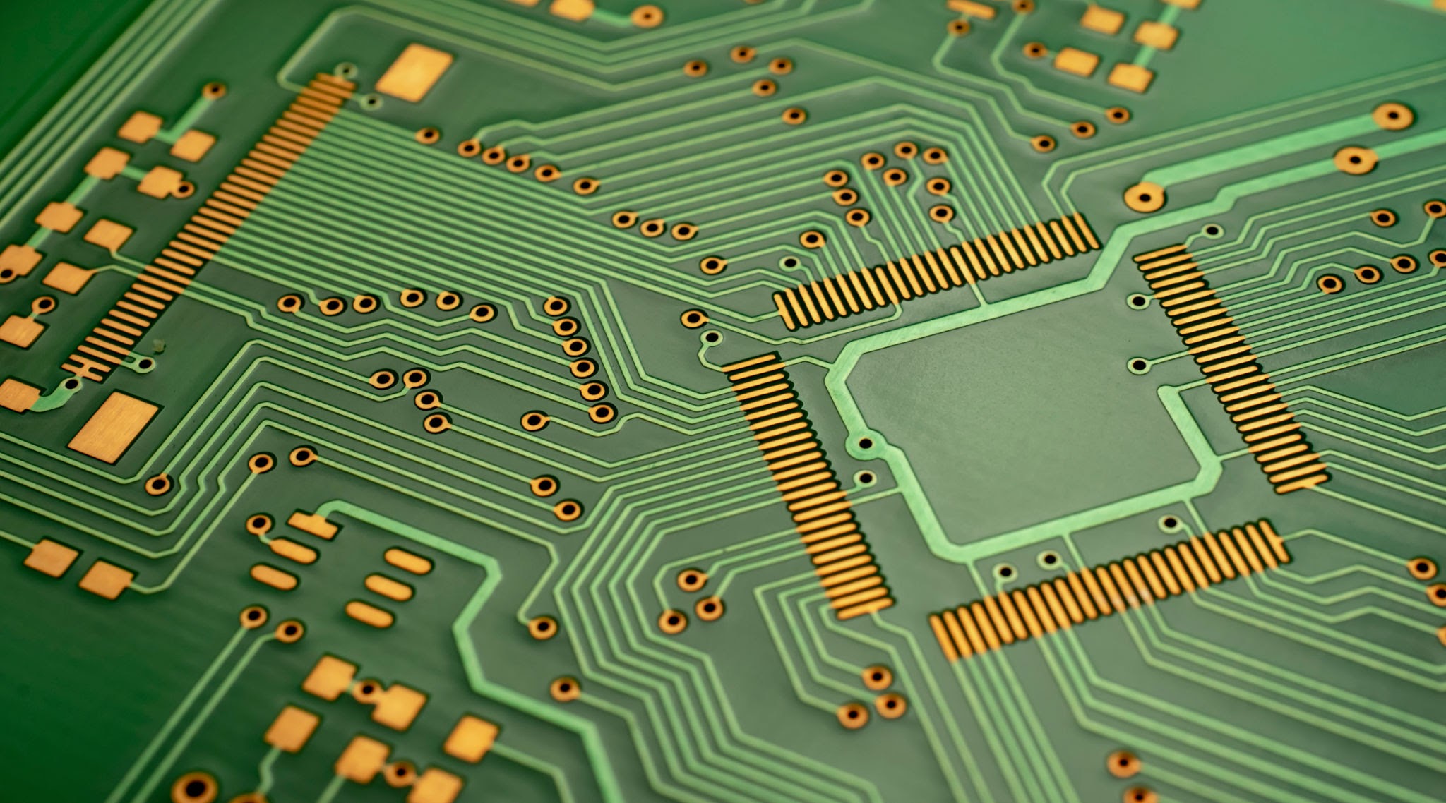
In the world of electronics manufacturing, there is a crucial component that often goes unnoticed but plays a vital role in powering the devices we rely on daily. Printed Circuit Boards (PCBs) serve as the backbone of modern electronics, providing the necessary platform for the intricate interconnections that bring electronic components to life. Behind the scenes, there is a complex and meticulous manufacturing process involved in creating these essential circuit boards.

At the forefront of this manufacturing process is the 569th Electronics Maintenance Squadron Circuit Board Manufacturing Shop, an integral part of providing combat-ready avionics parts and services to the warfighter. Located at the Warner Robins Air Logistics Complex, 402nd Electronics Maintenance Group in Robins Air Force Base, Georgia, this facility takes pride in its role in sustaining 75% of the Air Force organic workload.

Led by Bob Hillis, the supervisor of the 569th EMXS Circuit Board Manufacturing Shop, a dedicated team of ten individuals operates one of the two circuit board printing shops in the Department of Defense. Their primary focus lies in producing a wide array of printed circuit boards, including rigid, flex, multi-layer, single-sided, and double-sided designs, catering not only to the Air Force but also occasionally to other branches.

The manufacturing process commences with a thin sheet of laminate, which undergoes a series of intricate steps to transform it into a fully functional circuit board. Hillis explains that the process involves plating, drilling, imaging, development, stripping, and etching, as well as pressing and inspection, among other crucial steps. Each of these steps requires careful precision and adherence to strict production guidelines to ensure the highest quality standards are met.
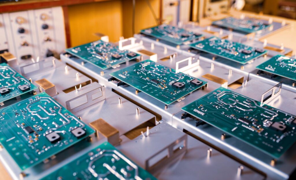
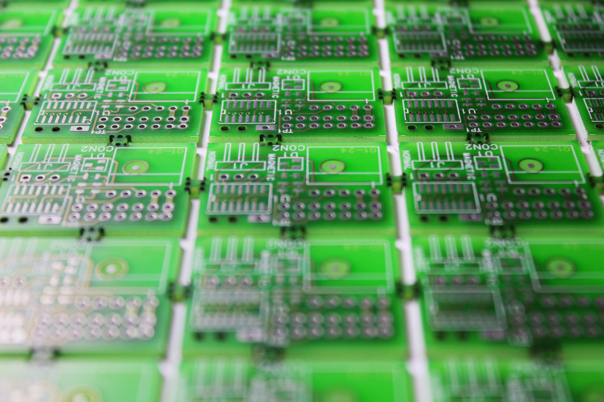
PCB manufacturing company
Microcircuits and components lie on metal plates during the production of super modern military computers and spy equipment. Concept of a secret military factory

One particularly fascinating aspect of their work lies in the production of circuit boards for heavy lift trailers used to load bombers. These trailers, some of which have been in service for over 45 years, are a critical part of maintaining the U.S. Air Force bomber fleet’s nuclear and conventional mission. The 569th EMXS Circuit Board Manufacturing Shop is actively involved in their service life extension program, manufacturing the necessary circuit cards to update and enhance these trailers. For the 196-type trailers, 133 circuit cards are required, while the 204-type trailers call for 32 completed cards.
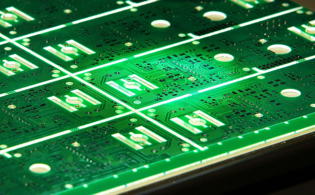
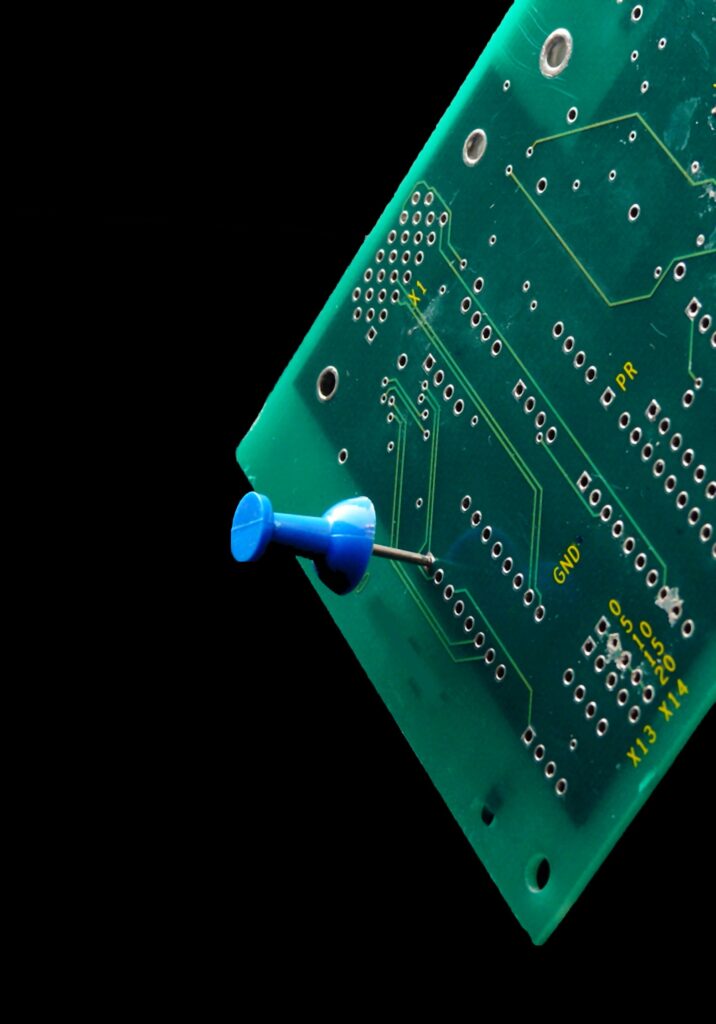
Printed circuit board

To stay at the forefront of the circuit board industry, the team at the 569th EMXS Circuit Board Manufacturing Shop emphasizes continuous training and improvement. Regularly attending conferences, seminars, and training sessions, they strive to enhance their processes and remain up-to-date with the latest advancements in the field. This commitment to ongoing education ensures that they are equipped with the necessary knowledge and skills to deliver high-quality circuit boards that meet the demanding standards of the military.

Manufacturing printed circuit boards for the nation’s military is a responsibility that the team takes great pride in. Hillis acknowledges the weight of their role but finds immense satisfaction in knowing that their work contributes to critical assets for global warfighters. Whether manufacturing new circuit boards or repairing existing ones, the 569th EMXS Circuit Board Manufacturing Shop recognizes the honor and importance of their contribution to the defense and security of the nation.

While the manufacturing process of PCBs may be hidden from the eyes of the end consumer, it is a fascinating journey of precision and expertise. From the initial stages of plating and drilling to the final inspection and testing, each step is a testament to the skill and dedication of the individuals involved. As we continue to rely on increasingly advanced electronics in our daily lives, let us not forget the intricate manufacturing process behind the circuit boards that power our devices and shape the world of technology.
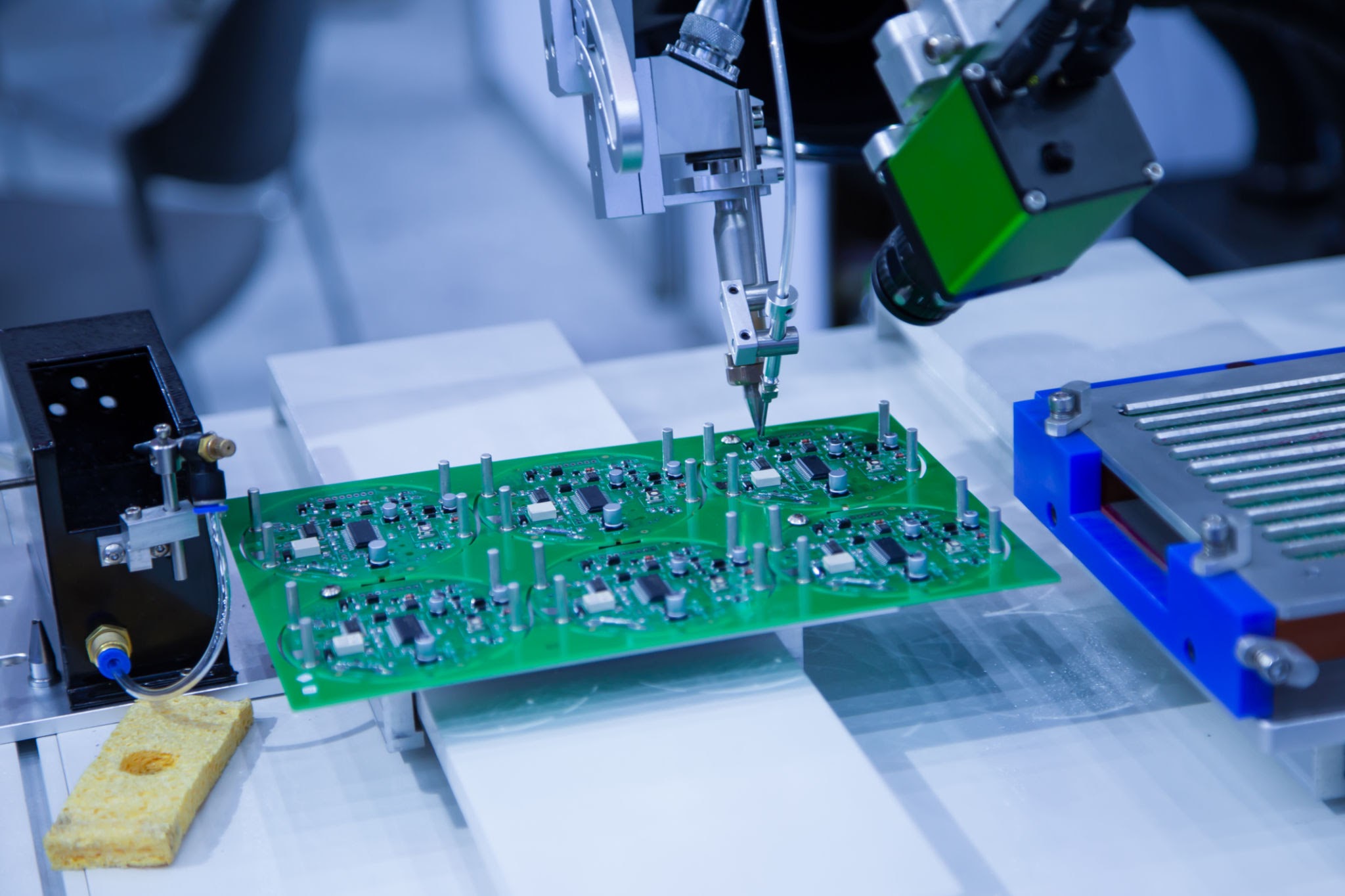
Essential Machinery for PCB Production: Protection Act Compliance

The U.S. “Protection of Circuit Boards and Substrates Act” is a crucial piece of legislation that aims to safeguard the integrity and security of circuit boards and substrates used in various electronic devices. With the increasing demand for advanced electronic products, many businesses in the United States are considering expanding or building PCB production lines. In this blog, we will provide an interpretation of the Protection of Circuit Boards and Substrates Act, and delve into the essential machinery required in a PCB production line, including PCB etching machines, PCB cleaning machines, PCB drilling machines, PCB browning machines, PCB sandblasting machines, PCB polishing machines, PCB oxidation resistance machines, PCB desoldering machines, PCB stripping machines, and PCB developing exposing machines. This information will help visitors who are motivated to purchase these machines and establish or expand their own PCB production lines.

The “Protection of Circuit Boards and Substrates Act” is a significant legislation aimed at ensuring the security and integrity of circuit boards and substrates used in electronic devices within the United States. The act recognizes the critical role played by circuit boards and substrates in the functioning of electronic products and seeks to prevent unauthorized modifications, counterfeiting, and tampering that could compromise their performance or pose security risks.

The act encompasses various provisions and requirements that manufacturers, distributors, and users of circuit boards and substrates must adhere to in order to comply with the law. Some key aspects of the act include:

  1. Counterfeit Prevention: The act emphasizes the need to combat the production and distribution of counterfeit circuit boards and substrates. It prohibits the manufacturing, sale, or use of counterfeit components and mandates stringent measures to ensure the authenticity of these critical electronic parts.
  2. Traceability and Documentation: The act emphasizes the importance of traceability and documentation throughout the supply chain. Manufacturers and distributors are required to maintain detailed records of the origin, manufacturing process, and distribution of circuit boards and substrates. This information helps establish accountability and facilitates effective quality control and product recalls if necessary.
  3. Quality Assurance: The act promotes the implementation of rigorous quality assurance measures throughout the production process. Manufacturers are encouraged to adopt industry best practices and adhere to recognized standards to ensure the reliability, performance, and safety of circuit boards and substrates.
  4. Security Measures: The act recognizes the need to safeguard electronic devices against potential security threats. It encourages the use of secure designs, authentication mechanisms, and encryption technologies to protect the integrity of circuit boards and substrates. This is particularly relevant in applications where the confidentiality of data or critical operations are at stake.
  5. Compliance and Enforcement: The act establishes mechanisms for compliance verification and enforcement. Regulatory authorities are empowered to conduct inspections, audits, and investigations to ensure that manufacturers and distributors are in compliance with the provisions of the act. Non-compliance can result in penalties, fines, or other legal consequences.

The “Protection of Circuit Boards and Substrates Act” reflects the growing importance of circuit boards and substrates in today’s interconnected and technology-driven world. By establishing guidelines and regulations, the act aims to foster trust among consumers and businesses, protect intellectual property, and promote the safe and reliable use of electronic devices.

For businesses involved in the establishment or expansion of PCB production lines, understanding and adhering to the requirements outlined in the act is essential. Compliance with the act not only ensures legal adherence but also demonstrates a commitment to quality, security, and customer satisfaction.

The Protection of Circuit Boards and Substrates Act focuses on safeguarding the manufacturing, distribution, and use of circuit boards and substrates within the United States. The act imposes regulations to prevent counterfeiting, tampering, and unauthorized modifications to these critical components, ensuring the reliability and security of electronic devices. It is important for businesses engaged in PCB production to adhere to the requirements specified in this act to maintain compliance with the law and protect consumer trust.

Customized PCB production line for customers: A Customer Case Study #etching #cleaning #sandblasting
Dragon Etching Customized PCB production line for customers

Dragon Etching Essential Machinery in a PCB Production Line:

  • PCB Etching Machine: PCB etching machines are vital in the production process as they facilitate the removal of unwanted copper from the substrate, creating the desired circuitry. These machines use chemical processes to dissolve the excess copper, leaving behind the required copper traces for circuit connections.
  • PCB Cleaning Machine: PCB cleaning machines are used to remove any contaminants or residues that accumulate during the manufacturing process. They employ various cleaning methods such as ultrasonic cleaning, brush cleaning, and chemical cleaning to ensure the cleanliness and reliability of the circuit boards.
  • PCB Drilling Machine: PCB drilling machines are responsible for creating holes in the circuit boards to accommodate electronic components. These machines utilize high-speed rotating drill bits to accurately drill holes of varying sizes, ensuring precise placement and alignment.
  • PCB Browning Machine: PCB browning machines, also known as brown oxide machines, are used to create a protective layer on the exposed copper surfaces of the circuit boards. This layer prevents oxidation and enhances the conductivity of the copper traces, improving the overall performance and longevity of the PCB.
  • PCB Sandblasting Machine: PCB sandblasting machines are employed for surface preparation, primarily to remove solder mask or copper from specific areas. This process is crucial for creating solder pads and ensuring proper solder adhesion during component assembly.
  • PCB Polishing Machine: PCB polishing machines are used to refine the surface finish of circuit boards. They remove any imperfections, such as rough edges or burrs, resulting from the manufacturing process, and provide a smooth and uniform surface for further processing or component placement.
  • PCB Oxidation Resistance Machine: PCB oxidation resistance machines apply protective coatings to the circuit boards, safeguarding them against environmental factors such as humidity, moisture, and corrosive substances. These coatings enhance the reliability and durability of the PCBs, ensuring their longevity in demanding applications.
  • PCB Desoldering Machine: PCB desoldering machines are essential for repairing or reworking PCBs. They allow the removal of electronic components without damaging the board, enabling efficient repairs and replacements during the production process or after device assembly.
  • PCB Stripping Machine: PCB stripping machines are used to remove unwanted solder masks, ensuring accurate solder pad exposure

Revolutionizing PCB Manufacturing: How MacroFab’s Innovative Approach and Advanced Technology are Changing the Game

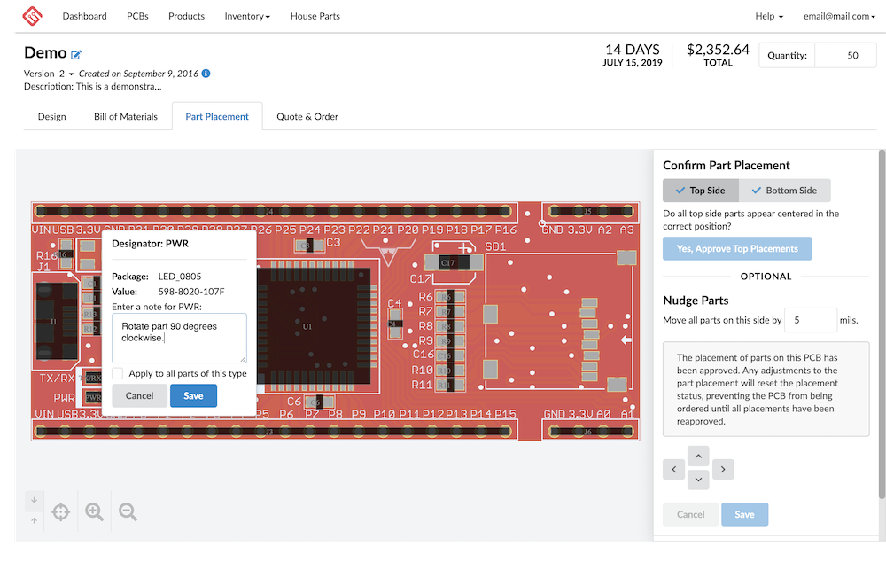
Printed Circuit Board (PCB) manufacturing has become an essential part of the manufacturing industry as electronic devices continue to proliferate. In recent years, the digital transformation of the manufacturing industry has brought significant opportunities and challenges to the PCB manufacturing sector. MacroFab, a company that specializes in PCB assembly, is at the forefront of this transformation, providing cutting-edge solutions to meet the growing demands of the industry.

MacroFab’s innovative approach to PCB assembly includes the use of automated assembly lines, advanced software, and machine learning algorithms. These technologies allow the company to produce high-quality PCBs with greater efficiency and precision than traditional manufacturing methods. The automated assembly lines, for example, can handle high volumes of PCBs with minimal human intervention, reducing the likelihood of errors and increasing production speed.

The use of advanced software and machine learning algorithms also allows MacroFab to optimize its manufacturing processes. By analyzing data on production processes and identifying areas of inefficiency, the company can improve its operations and reduce costs. This, in turn, allows MacroFab to offer its customers competitive pricing while maintaining high-quality standards.

Another advantage of MacroFab’s approach to PCB assembly is its ability to customize its solutions to meet the specific needs of its customers. Whether it’s a small-scale project or a large-scale production run, MacroFab can tailor its services to meet the unique requirements of each customer. This flexibility is essential in today’s fast-paced manufacturing industry, where agility and responsiveness are crucial for success.

In conclusion, the digital transformation of the manufacturing industry has brought significant changes to the PCB manufacturing sector, and companies like MacroFab are leading the way in this transformation. With their innovative approach to PCB assembly, advanced technologies, and customer-centric approach, MacroFab is well-positioned to meet the growing demands of the industry and help shape its future.

As a manufacturer of PCB etching machines, you understand the critical role that this equipment plays in the manufacturing process. With the increasing demand for electronic devices, the need for high-quality PCBs has never been greater. MacroFab, a leading company in the PCB assembly industry, has demonstrated how innovative solutions and advanced technology can meet this demand while providing cost-effective solutions for its customers.

MacroFab’s use of automated assembly lines, advanced software, and machine learning algorithms has revolutionized the PCB assembly process. By automating the assembly process, MacroFab can handle high volumes of PCBs with minimal human intervention, reducing the risk of errors and increasing production speed. The use of advanced software and machine learning algorithms allows MacroFab to optimize its manufacturing processes by analyzing data and identifying areas of inefficiency.

The company’s customer-centric approach allows it to customize its services to meet the specific needs of each customer, from small-scale projects to large-scale production runs. This flexibility is crucial in today’s fast-paced manufacturing industry, where agility and responsiveness are essential for success.

As a PCB etching machine manufacturer, you can learn from MacroFab’s success and apply their principles to your business. By investing in innovative solutions and advanced technology, you can improve the efficiency and precision of your machines, providing cost-effective solutions for your customers. Additionally, you can adopt a customer-centric approach, providing customized services that meet the unique needs of your customers.

In conclusion, the case of MacroFab’s success in the PCB assembly industry provides valuable lessons for PCB etching machine manufacturers. By investing in innovation and advanced technology and adopting a customer-centric approach, you can differentiate your business and provide high-quality, cost-effective solutions for your customers. As the demand for electronic devices continues to grow, it’s essential to position yourself as a leader in the industry, providing solutions that meet the needs of your customers and help shape the future of PCB manufacturing.

Conclusion: The digital transformation of the manufacturing industry has brought significant changes to the PCB manufacturing sector. The success of MacroFab in the PCB assembly industry provides valuable lessons for PCB etching machine manufacturers. By embracing innovation and a customer-centric approach, manufacturers can differentiate themselves and provide high-quality, cost-effective solutions for their customers. As the demand for electronic devices continues to grow, it is essential to position oneself as a leader in the industry, providing solutions that meet the needs of customers and help shape the future of PCB manufacturing.

What to Make of U.S. Government Will Support Domestic PCB Manufacturing

The United States government is taking initiatives to support domestic manufacturing of printed circuit boards (PCBs). The move is aimed at promoting technological self-sufficiency and reducing dependence on foreign manufacturing. This report will discuss the challenges faced by the domestic PCB manufacturing industry and the government’s efforts to support it.

U.S. Government Will Support Domestic PCB Manufacturing

Challenges faced by domestic PCB manufacturing industry: The domestic PCB manufacturing industry has faced several challenges in recent years, including competition from cheaper imports, lack of investment in research and development, and the high cost of manufacturing equipment. This has resulted in a decline in the number of domestic PCB manufacturers and a growing dependence on foreign manufacturers.

Government’s initiatives to support domestic PCB manufacturing: The U.S. government has announced several initiatives to support domestic PCB manufacturing. One such initiative is the creation of a public-private partnership called the American Institute for Manufacturing of Advanced PCBs (AIM Photonics). This partnership aims to provide funding for research and development of advanced technologies, such as high-density interconnect (HDI) PCBs, which are commonly used in advanced packaging applications.

The government has also announced a plan to provide financial incentives for domestic PCB manufacturers to invest in new equipment and technology. The incentives are expected to make it easier for domestic manufacturers to purchase new equipment and upgrade their facilities, thus making them more competitive in the global market.

Additionally, the government plans to establish a network of advanced manufacturing institutes across the country that will focus on developing and implementing advanced manufacturing technologies, including PCB manufacturing. These institutes will provide technical support and training to domestic manufacturers, enabling them to develop and adopt new manufacturing techniques and technologies.

Conclusion: The government’s efforts to support domestic PCB manufacturing are a welcome move that will help promote technological self-sufficiency and reduce dependence on foreign manufacturers. By providing funding for research and development of advanced technologies and financial incentives for domestic manufacturers, the government is helping to create a more competitive domestic PCB manufacturing industry. The establishment of advanced manufacturing institutes across the country will also provide technical support and training to domestic manufacturers, helping them to stay up-to-date with the latest manufacturing techniques and technologies.

What technical support is required for packaging PCB?

To package PCBs, a variety of technical support is required, including:

  • Design software: Packaging PCBs requires specialized design software that can create and test the packaging design before it goes into production. This software must be able to create 3D models of the PCB, generate the necessary manufacturing files, and perform simulations to ensure the design meets the required specifications.
  • Manufacturing equipment: Once the PCB packaging design is finalized, it needs to be manufactured. This requires specialized equipment, such as pick-and-place machines, soldering equipment, and testing equipment, to assemble the PCB components and test the final product.
  • Material selection: Selecting the right materials is critical to ensuring the PCB packaging meets the required specifications. Technical support is required to help choose the right materials based on factors such as the operating environment, durability, and electrical properties.
  • Thermal management: PCBs generate heat, and packaging design needs to include thermal management strategies to ensure the PCB doesn’t overheat. Technical support is required to help determine the best thermal management strategy, including heat sinks, fans, and other cooling methods.
  • Compliance testing: The PCB packaging design needs to meet various regulatory requirements and industry standards. Technical support is required to ensure the design meets these standards and passes compliance testing.

Overall, packaging PCBs requires a significant amount of technical expertise and support to ensure the final product meets the required specifications and performs as intended.

PCB Production Process: A Complete Guide to Designing and Manufacturing Machines Electronic Circuits

Printed Circuit Boards (PCBs) are an essential component of modern electronic devices. PCBs provide a means of interconnecting electronic components, enabling the creation of complex and sophisticated electronic systems. The production of PCBs involves a series of steps that require precision, expertise, and specialized equipment. In this blog post, we will discuss the PCB production process in detail.

PCB Design:

The first step in the production of PCBs is the design phase. During this phase, engineers use computer-aided design (CAD) software to create a schematic diagram and a physical layout of the circuit. The circuit layout is the blueprint for the final product, and it determines the placement of electronic components and the routing of electrical connections.

PCB Manufacturing:

Once the circuit layout is finalized, the PCB manufacturing process can begin. The circuit layout is printed on a copper-clad board using a process called etching. The board is coated with a layer of photoresist, which is then exposed to UV light through a stencil of the circuit layout. The unexposed areas of the photoresist are then dissolved, leaving behind a pattern of copper on the board. This pattern of copper traces makes up the circuit.

Dragon Etching: Inside Look at PCB Manufacturing,test, from Workshop to Shipping | Sunset Delivery
PCB etching machine plants

PCB Etching:

Etching is the process of removing unwanted copper from the PCB to create the desired circuit pattern. It is done by exposing the board to an etchant, which selectively removes the copper from the areas not protected by the photoresist. After the etching process is complete, the remaining photoresist is stripped away, leaving behind the desired circuit pattern.

Home
PCB Etching Machine

PCB Developing Exposing:

The board is then developed using a chemical solution that dissolves the exposed photoresist, leaving behind the copper pattern that makes up the circuit. This process is known as developing.

Home
PCB Developing Exposing Machine

PCB Stripping:

Once the copper pattern is developed, the remaining photoresist must be stripped away using a chemical solution, leaving only the copper traces behind. This process is known as stripping.

Home
PCB Stripping Machine

PCB Cleaning:

After stripping, the board is thoroughly cleaned to remove any chemical residue and ensure a clean surface for the next step.

Home
PCB Cleaning Machine

PCB Desoldering:

During the assembly process, electronic components may need to be removed or replaced, requiring desoldering. This is done using specialized tools and techniques to remove the solder holding the component in place without damaging the board or the component.

Home
PCB Desoldering Machine

PCB Oxidation Resistance:

PCBs are susceptible to oxidation, which can cause corrosion and damage to the board over time. To prevent this, a layer of oxidation-resistant material is applied to the board to protect it from the environment.

Home
PCB Oxidation Resistance Machine

PCB Polishing:

Home
PCB Polishing Machine

After the oxidation-resistant layer is applied, the board may be polished to create a smooth surface and ensure the proper thickness of the copper traces.

PCB Sandblasting:

In some cases, the board may be sandblasted to create a rough surface for improved adhesion of the oxidation-resistant material.

Home
PCB Sandblasting Machine

PCB Browning:

Finally, the board may be treated with a chemical solution to create a brown or black surface that provides a contrast for easier inspection and testing.

In conclusion, the production of PCBs involves a series of steps that require precision, expertise, and specialized equipment. The PCB production process is critical to the functioning and performance of electronic devices, and it must be executed with care and attention to detail.

Home
PCB Browning Machine