Discover the complex steps involved in creating printed circuit boards (PCBs) and their vital role in powering modern electronics.
The Intricate Manufacturing Process of PCBs: Building the Backbone of Modern Electronics
In the world of electronics manufacturing, there is a crucial component that often goes unnoticed but plays a vital role in powering the devices we rely on daily. Printed Circuit Boards (PCBs) serve as the backbone of modern electronics, providing the necessary platform for the intricate interconnections that bring electronic components to life. Behind the scenes, there is a complex and meticulous manufacturing process involved in creating these essential circuit boards.
At the forefront of this manufacturing process is the 569th Electronics Maintenance Squadron Circuit Board Manufacturing Shop, an integral part of providing combat-ready avionics parts and services to the warfighter. Located at the Warner Robins Air Logistics Complex, 402nd Electronics Maintenance Group in Robins Air Force Base, Georgia, this facility takes pride in its role in sustaining 75% of the Air Force organic workload.
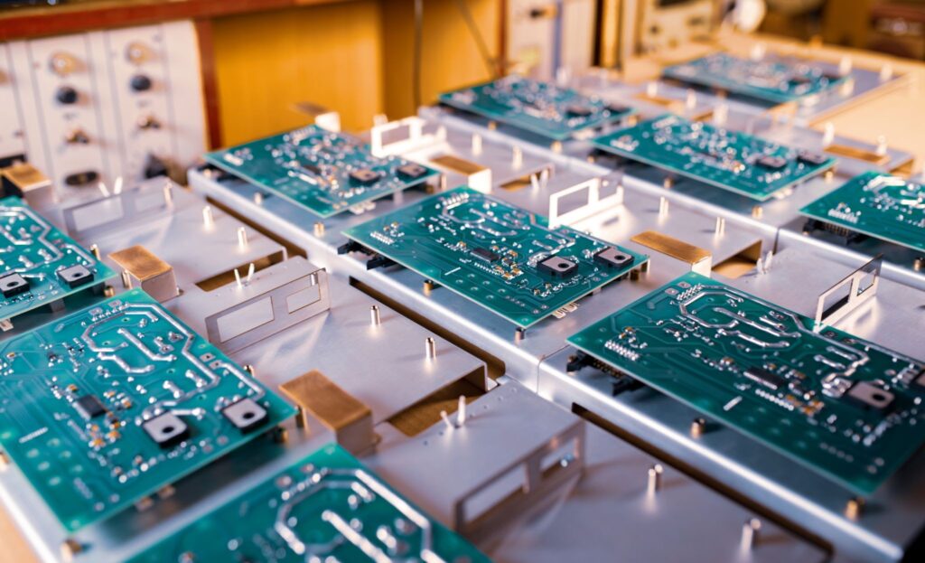
Led by Bob Hillis, the supervisor of the 569th EMXS Circuit Board Manufacturing Shop, a dedicated team of ten individuals operates one of the two circuit board printing shops in the Department of Defense. Their primary focus lies in producing a wide array of printed circuit boards, including rigid, flex, multi-layer, single-sided, and double-sided designs, catering not only to the Air Force but also occasionally to other branches.
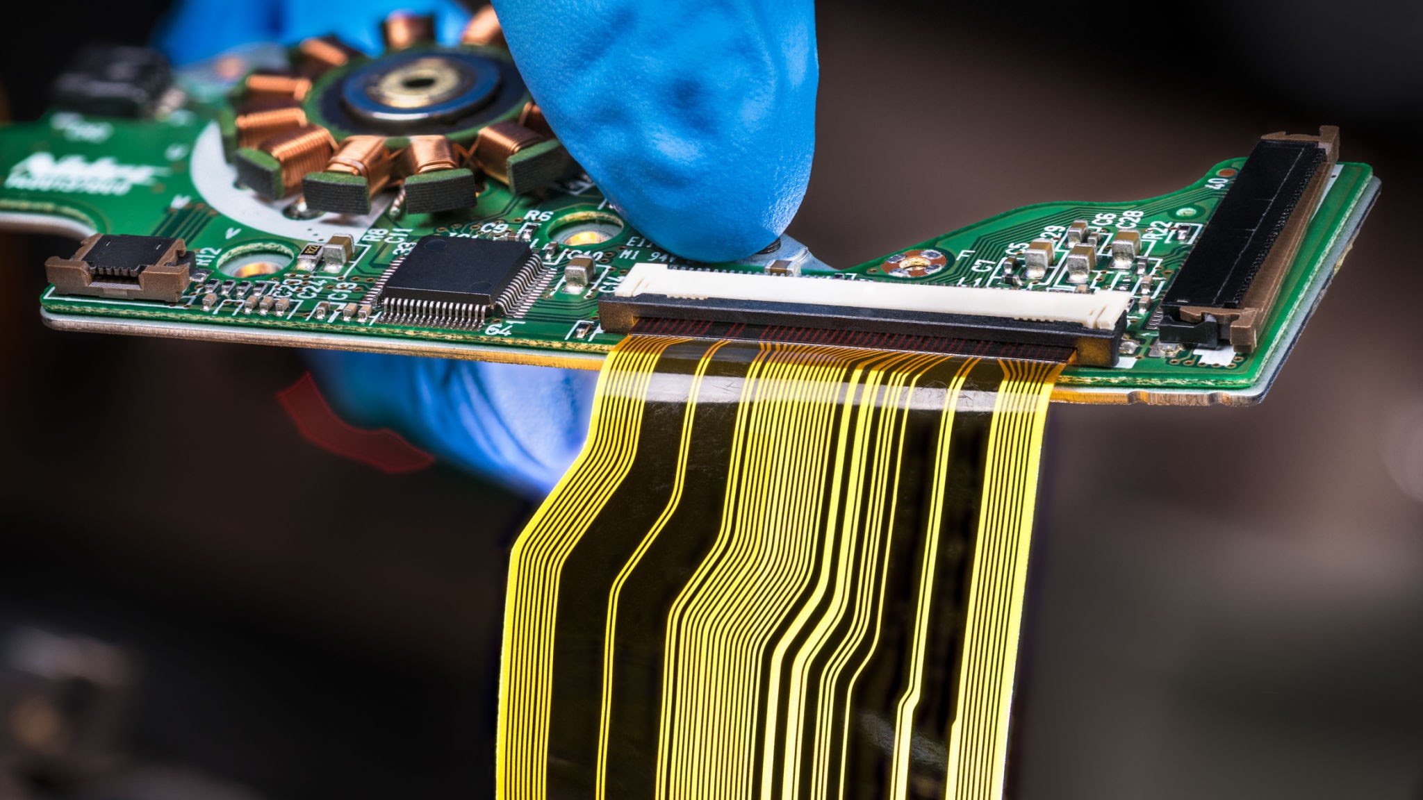
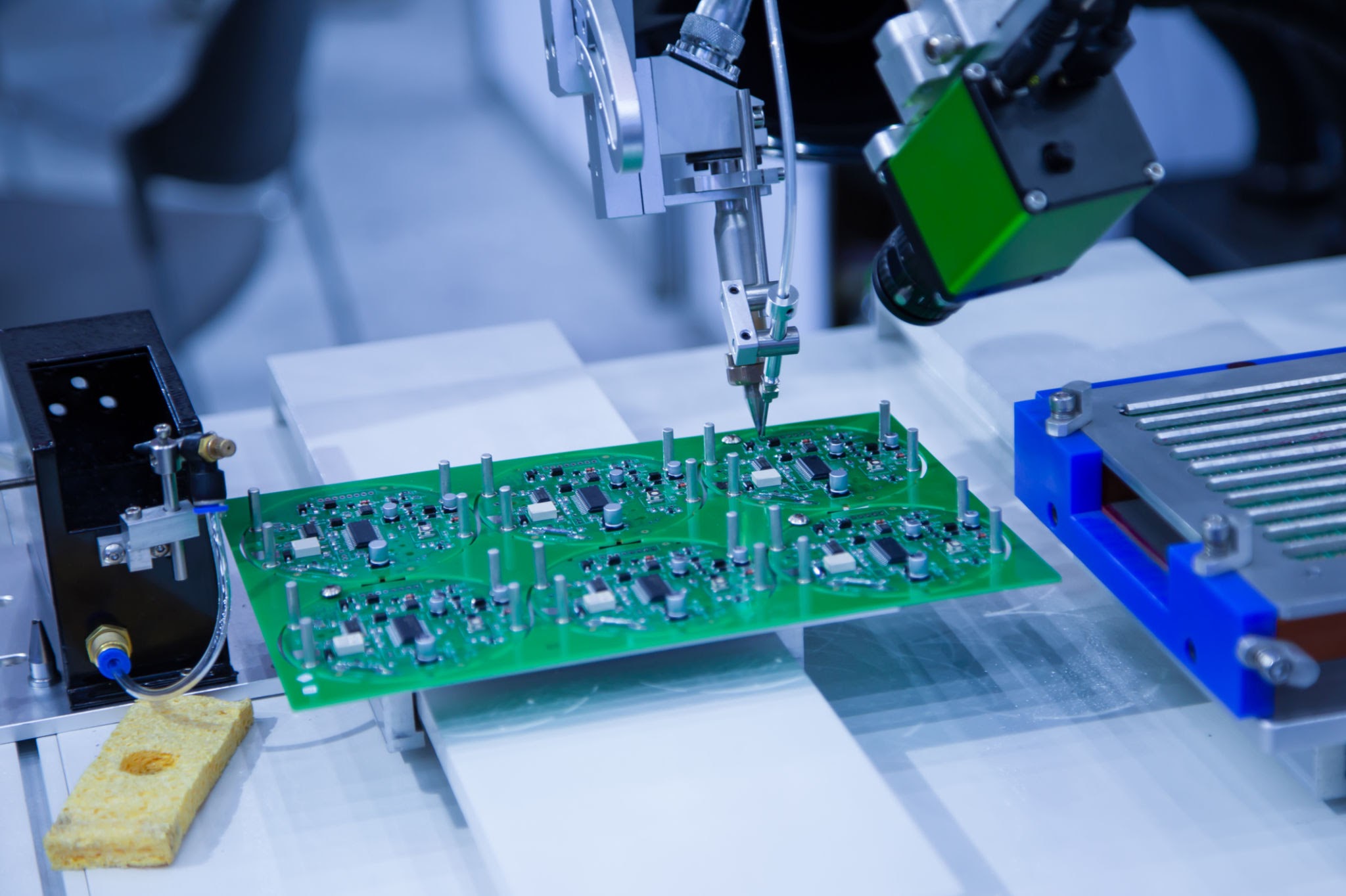
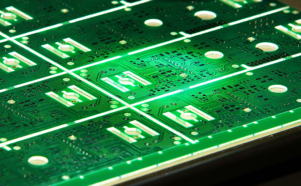
The manufacturing process commences with a thin sheet of laminate, which undergoes a series of intricate steps to transform it into a fully functional circuit board. Hillis explains that the process involves plating, drilling, imaging, development, stripping, and etching, as well as pressing and inspection, among other crucial steps. Each of these steps requires careful precision and adherence to strict production guidelines to ensure the highest quality standards are met.
One particularly fascinating aspect of their work lies in the production of circuit boards for heavy lift trailers used to load bombers. These trailers, some of which have been in service for over 45 years, are a critical part of maintaining the U.S. Air Force bomber fleet’s nuclear and conventional mission. The 569th EMXS Circuit Board Manufacturing Shop is actively involved in their service life extension program, manufacturing the necessary circuit cards to update and enhance these trailers. For the 196-type trailers, 133 circuit cards are required, while the 204-type trailers call for 32 completed cards.
To stay at the forefront of the circuit board industry, the team at the 569th EMXS Circuit Board Manufacturing Shop emphasizes continuous training and improvement. Regularly attending conferences, seminars, and training sessions, they strive to enhance their processes and remain up-to-date with the latest advancements in the field. This commitment to ongoing education ensures that they are equipped with the necessary knowledge and skills to deliver high-quality circuit boards that meet the demanding standards of the military.
Manufacturing printed circuit boards for the nation’s military is a responsibility that the team takes great pride in. Hillis acknowledges the weight of their role but finds immense satisfaction in knowing that their work contributes to critical assets for global warfighters. Whether manufacturing new circuit boards or repairing existing ones, the 569th EMXS Circuit Board Manufacturing Shop recognizes the honor and importance of their contribution to the defense and security of the nation.
While the manufacturing process of PCBs may be hidden from the eyes of the end consumer, it is a fascinating journey of precision and expertise. From the initial stages of plating and drilling to the final inspection and testing, each step is a testament to the skill and dedication of the individuals involved. As we continue to rely on increasingly advanced electronics in our daily lives, let us not forget the intricate manufacturing process behind the circuit boards that power our devices and shape the world of technology.