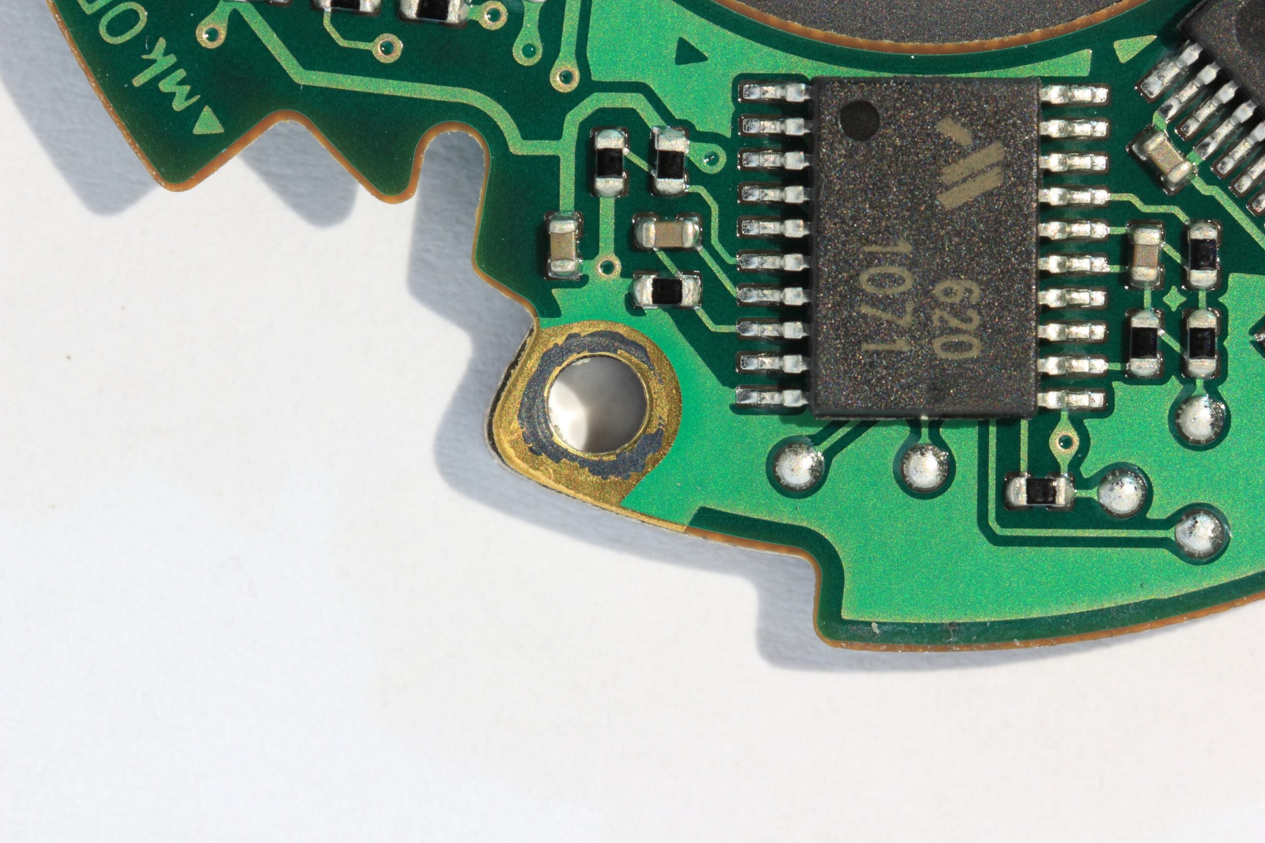
Printed Circuit Boards (PCBs) are an essential component of modern electronic devices. PCBs provide a means of interconnecting electronic components, enabling the creation of complex and sophisticated electronic systems. The production of PCBs involves a series of steps that require precision, expertise, and specialized equipment. In this blog post, we will discuss the PCB production process in detail.
PCB Design:
The first step in the production of PCBs is the design phase. During this phase, engineers use computer-aided design (CAD) software to create a schematic diagram and a physical layout of the circuit. The circuit layout is the blueprint for the final product, and it determines the placement of electronic components and the routing of electrical connections.
PCB Manufacturing:
Once the circuit layout is finalized, the PCB manufacturing process can begin. The circuit layout is printed on a copper-clad board using a process called etching. The board is coated with a layer of photoresist, which is then exposed to UV light through a stencil of the circuit layout. The unexposed areas of the photoresist are then dissolved, leaving behind a pattern of copper on the board. This pattern of copper traces makes up the circuit.
PCB Etching:
Etching is the process of removing unwanted copper from the PCB to create the desired circuit pattern. It is done by exposing the board to an etchant, which selectively removes the copper from the areas not protected by the photoresist. After the etching process is complete, the remaining photoresist is stripped away, leaving behind the desired circuit pattern.
PCB Developing Exposing:
The board is then developed using a chemical solution that dissolves the exposed photoresist, leaving behind the copper pattern that makes up the circuit. This process is known as developing.
PCB Stripping:
Once the copper pattern is developed, the remaining photoresist must be stripped away using a chemical solution, leaving only the copper traces behind. This process is known as stripping.
PCB Cleaning:
After stripping, the board is thoroughly cleaned to remove any chemical residue and ensure a clean surface for the next step.
PCB Desoldering:
During the assembly process, electronic components may need to be removed or replaced, requiring desoldering. This is done using specialized tools and techniques to remove the solder holding the component in place without damaging the board or the component.
PCB Oxidation Resistance:
PCBs are susceptible to oxidation, which can cause corrosion and damage to the board over time. To prevent this, a layer of oxidation-resistant material is applied to the board to protect it from the environment.
PCB Polishing:
After the oxidation-resistant layer is applied, the board may be polished to create a smooth surface and ensure the proper thickness of the copper traces.
PCB Sandblasting:
In some cases, the board may be sandblasted to create a rough surface for improved adhesion of the oxidation-resistant material.
PCB Browning:
Finally, the board may be treated with a chemical solution to create a brown or black surface that provides a contrast for easier inspection and testing.
In conclusion, the production of PCBs involves a series of steps that require precision, expertise, and specialized equipment. The PCB production process is critical to the functioning and performance of electronic devices, and it must be executed with care and attention to detail.


