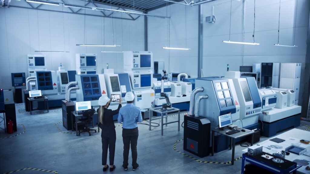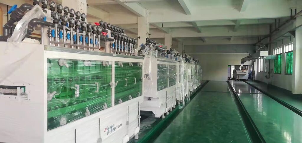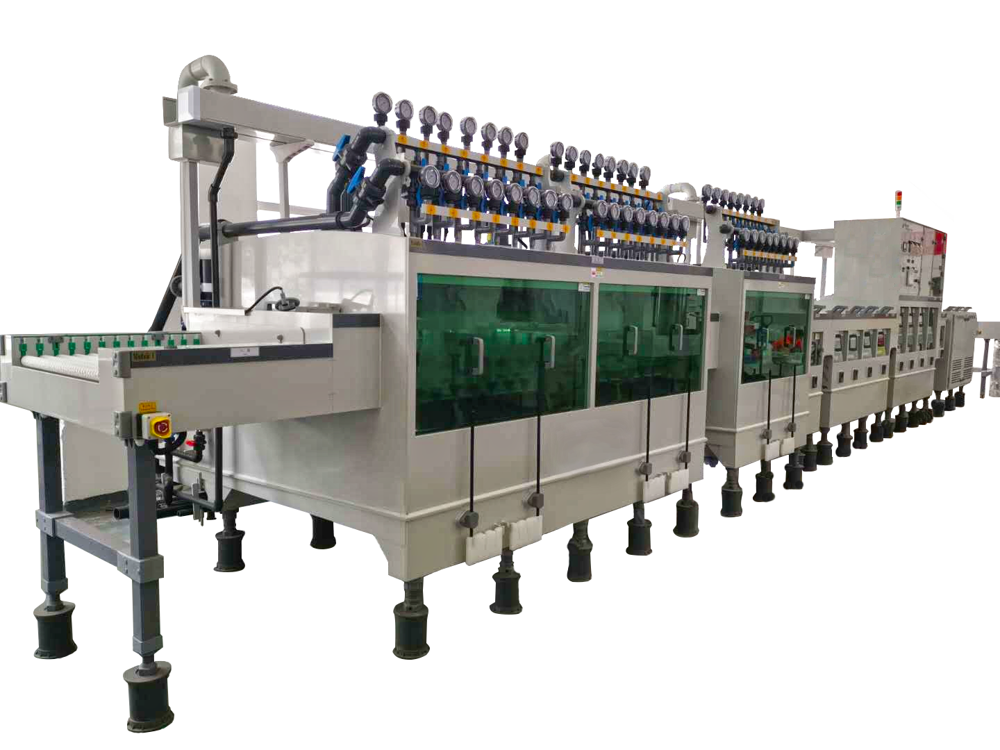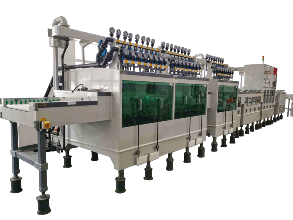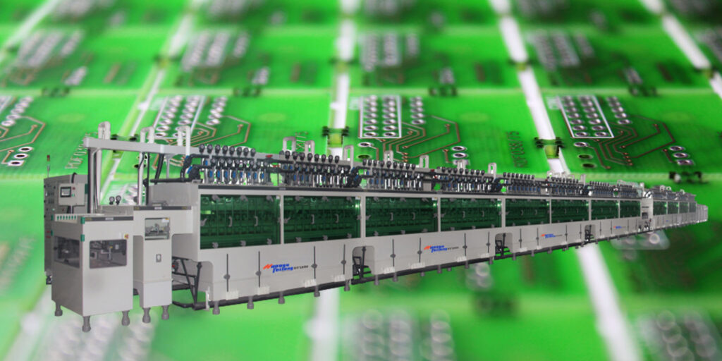
As the demand for high-density interconnects (HDI) continues to rise, the PCB industry is shifting towards next-generation developing machines designed to meet the requirements of increasingly complex circuit designs. These machines play a crucial role in the development of HDI boards, which feature fine lines, microvias, and high-density connections that are essential for modern electronic devices. To day will explore the microvia processing capabilities, HDI-compatible chemical systems, and the emerging technologies that enable the fabrication of high-performance, miniaturized PCBs. Specifically, we will cover advanced material compatibility, laser-drilled microvia development, mSAP support, pulse-spray technology, and other innovations that are pushing the boundaries of PCB manufacturing.
Advanced Material Compatibility
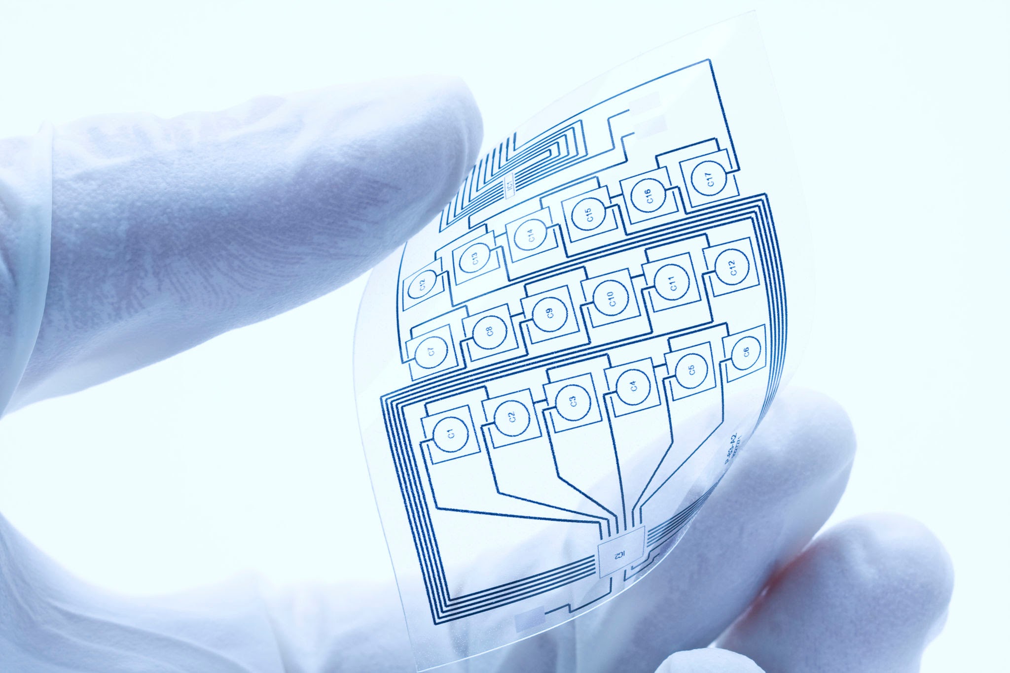
The development of HDI PCBs demands machines that can process advanced materials with precision and efficiency. As the designs become smaller and more intricate, the compatibility of PCB developing machines with various materials becomes increasingly important. Materials such as high-frequency laminates, flexible substrates, and ultra-thin cores require specialized systems to ensure they are processed correctly without compromising performance.
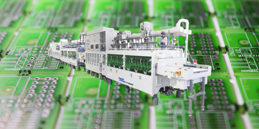
Laser Direct Imaging System From Han’s Laser

Achieve ultra-high efficiency solder mask processing, with up to 6 pieces/minute (24″x28″) for ordinary ink
Fully digitalized exposure process, entering the smart manufacturing of Industry 4.0
Equipped with high-quality high-power light source, enhance the polymerization reaction efficiency of solder mask ink
Independent unique high laser energy DMD control technology, enhance equipment reliability
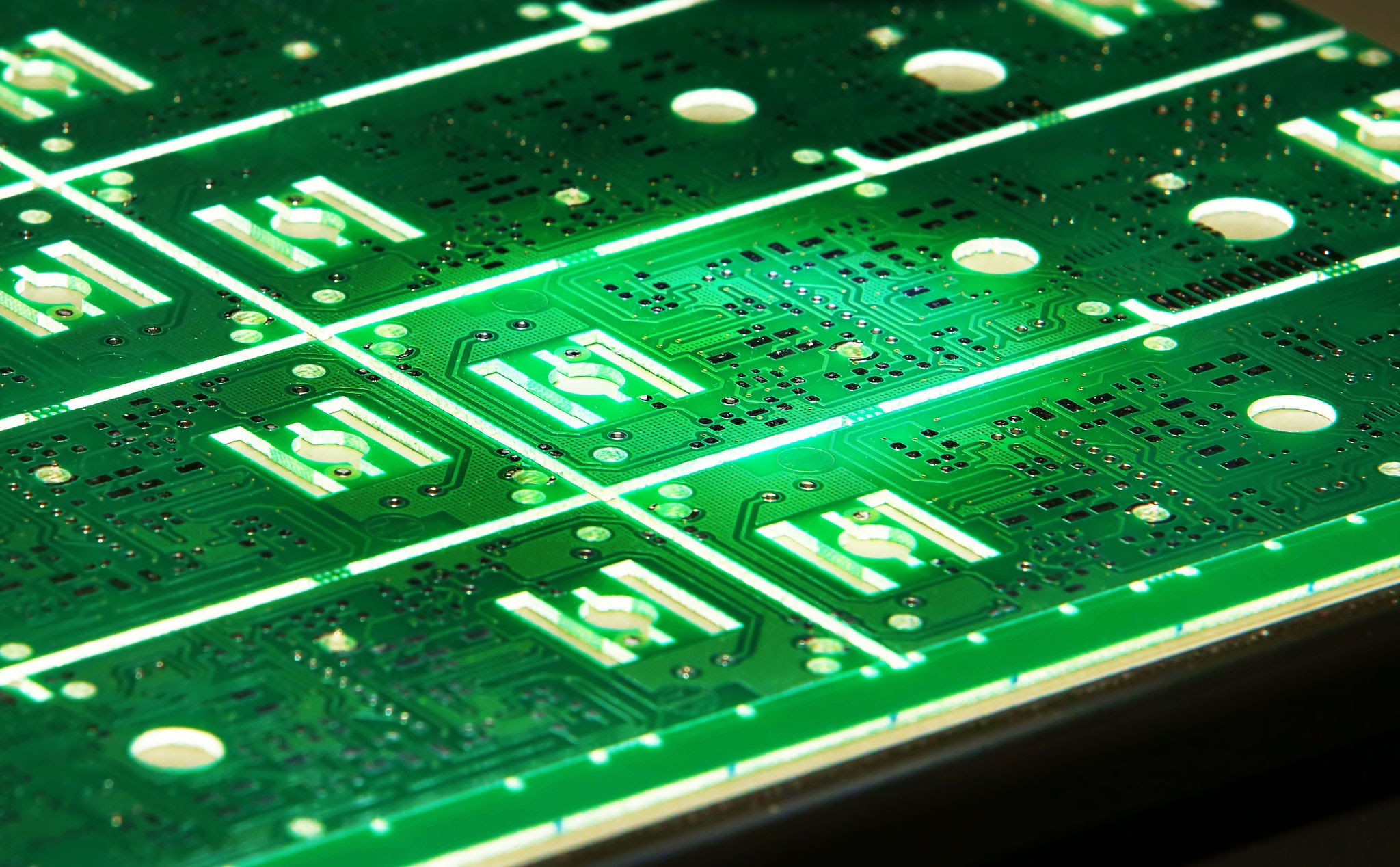
- Laser-drilled microvia development: Laser technology is increasingly used to drill microvias in HDI boards, offering superior precision and enabling the creation of finer vias that traditional mechanical methods cannot achieve. These machines need to be capable of handling the laser-ablated surface, ensuring that the chemical development process does not damage or compromise the via integrity.
- Low-roughness surface treatment: To achieve higher density and improved signal integrity, HDI boards require smooth, low-roughness surfaces for better copper plating and electrical performance. PCB developing machines must integrate advanced surface treatment capabilities to maintain these low-roughness profiles while ensuring reliable and uniform chemical processing.
Emerging Technology Integration
mSAP (Modified Semi-Additive Process) Support
One of the key technologies for producing high-density interconnects is mSAP, or the Modified Semi-Additive Process. This method allows for the creation of very fine traces and vias by combining additive and subtractive processes in PCB fabrication. Machines supporting mSAP must be able to handle ultra-fine feature definitions while ensuring that the chemical developer efficiently removes excess material.
With mSAP, selective copper plating is done only on the areas required, minimizing the copper thickness in non-essential areas, which is crucial for HDI applications. Developing machines that support this technology must deliver precise chemical application with a high degree of control, allowing for optimized plating and etching, which in turn leads to improved yield and reliability.
Ultra-Thin Core Processing Adaptations
In HDI boards, ultra-thin cores are often used to maintain compactness and high performance. These cores require careful handling during the development process to avoid damage. PCB developing machines need specialized adaptations to handle ultra-thin materials, ensuring uniform exposure to chemicals without excessive chemical etching or roughening.
Advanced machines use micro-spray nozzles or spray heads designed specifically for thin substrates, ensuring controlled chemical delivery and minimizing the risk of damage during the development process.
Process Window Expansion
As the complexity of PCB designs increases, so too does the need to expand the process window—the range of operating conditions under which the chemical development process can produce high-quality results. To meet the demands of high-density interconnect fabrication, next-gen machines incorporate several innovations:
Pulse-Spray Technology for Blind Vias
Pulse-spray technology is an emerging feature in PCB developing machines, specifically designed to handle blind vias in HDI PCBs. Blind vias are vias that do not extend all the way through the board, which poses a challenge for uniform chemical development. Pulse-spray technology involves applying pulses of developer fluid with precise volume control, allowing the machine to effectively process blind vias without over-developing the surrounding areas.
This technology enhances the development precision, ensuring that the entire via structure is properly treated, even in regions that are not fully accessible.

Variable Pressure Developer Delivery
Variable pressure developer delivery is another breakthrough technology for expanding the process window. By adjusting the pressure at which the developer is sprayed or delivered, this technology ensures that the chemical solution penetrates hard-to-reach areas of the PCB, including narrow vias and densely packed layers. The variable pressure allows for optimized chemical flow, improving the efficiency of development and reducing the risk of under or overdevelopment, particularly in fine-feature regions.
Future-Proof Design Features
As the electronics industry continues to demand more complex and miniaturized PCBs, PCB developing machines must be future-proof to remain competitive and adaptable to evolving technologies. Several key features are emerging that provide flexibility and scalability for PCB fabricators:
Modular Upgrade Pathways
To stay ahead of technological advancements, modern PCB developing machines are increasingly designed with modular upgrade pathways. These systems allow for easy hardware and software upgrades, ensuring that manufacturers can keep pace with new materials, emerging technologies, and changing industry standards without requiring a complete overhaul of their existing equipment. Whether it’s adding support for new chemistries, new development methods, or increased throughput, modularity provides manufacturers with the flexibility to adapt as needed.
Multi-Chemistry Reservoir Systems
The next generation of multi-chemistry reservoir systems enables PCB developing machines to process a variety of chemistries for different types of materials and processes. By incorporating multiple chemical reservoirs within a single system, these machines can seamlessly switch between chemistries tailored for different tasks, such as etching, plating, or microvia development, without the need for a full changeover.
These multi-chemistry systems enhance production flexibility and reduce downtime, allowing manufacturers to quickly switch between different types of PCBs—whether they are standard or high-density interconnects—without losing efficiency.

The evolving demands of high-density interconnect fabrication are driving the need for next-generation PCB developing machines. Innovations such as laser-drilled microvia processing, mSAP support, pulse-spray technology, and variable pressure developer delivery are critical for enabling the production of advanced, miniaturized PCBs with complex features.
By integrating advanced material compatibility, process window expansion, and future-proof design features, these machines provide manufacturers with the tools needed to meet the challenges of next-generation PCB production. With modular upgrade pathways and multi-chemistry reservoir systems, future PCB developers can ensure their systems remain adaptable to emerging technologies and maintain a competitive edge in the rapidly changing electronics industry.
The continued integration of emerging technologies and process innovations will ensure that PCB chemical developing machines remain at the forefront of high-density interconnect fabrication, offering the precision, flexibility, and scalability required for the future of electronics manufacturing.