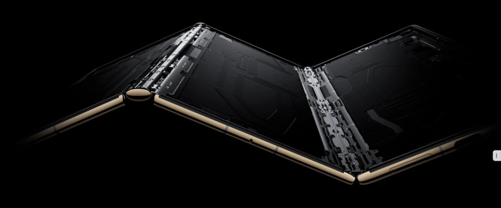
Explore the full process and equipment used for manufacturing Huawei Mate XT’s foldable screen and flexible PCBs. Learn about chemical etching, LDI exposure, developers, strippers, and cleaning machines crucial for producing high-precision flexible circuits.
To analyze the chemical etching equipment used in manufacturing the Huawei Mate XT’s folding screen and folding PCB, you can break down the process into two parts: screen etching and PCB etching.
1. Folding Screen Etching
The flexible display for foldable devices like the Huawei Mate XT likely involves etching processes for organic and inorganic materials used in OLED (Organic Light-Emitting Diode) or AMOLED displays. Here’s how etching plays a role:
- Materials Involved: The folding screen is typically made up of layers of organic compounds, thin metal films, and transparent conductive oxides (such as ITO – indium tin oxide).
- Etching Method: Wet chemical etching or dry etching (plasma or ion-beam) may be used to pattern the electrodes and define the screen areas. This allows precise control over layer removal for pixel definition, transparent circuits, and metal traces.
- Equipment:
- Wet chemical etching machines: These machines handle materials like ITO, which need precise etching to form conductive pathways.
- Dry etching equipment: For materials where plasma etching provides better control and sharper edges.
The etching must ensure uniformity and accuracy without damaging the flexible nature of the screen.
2. Folding PCB Etching
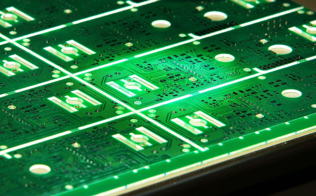
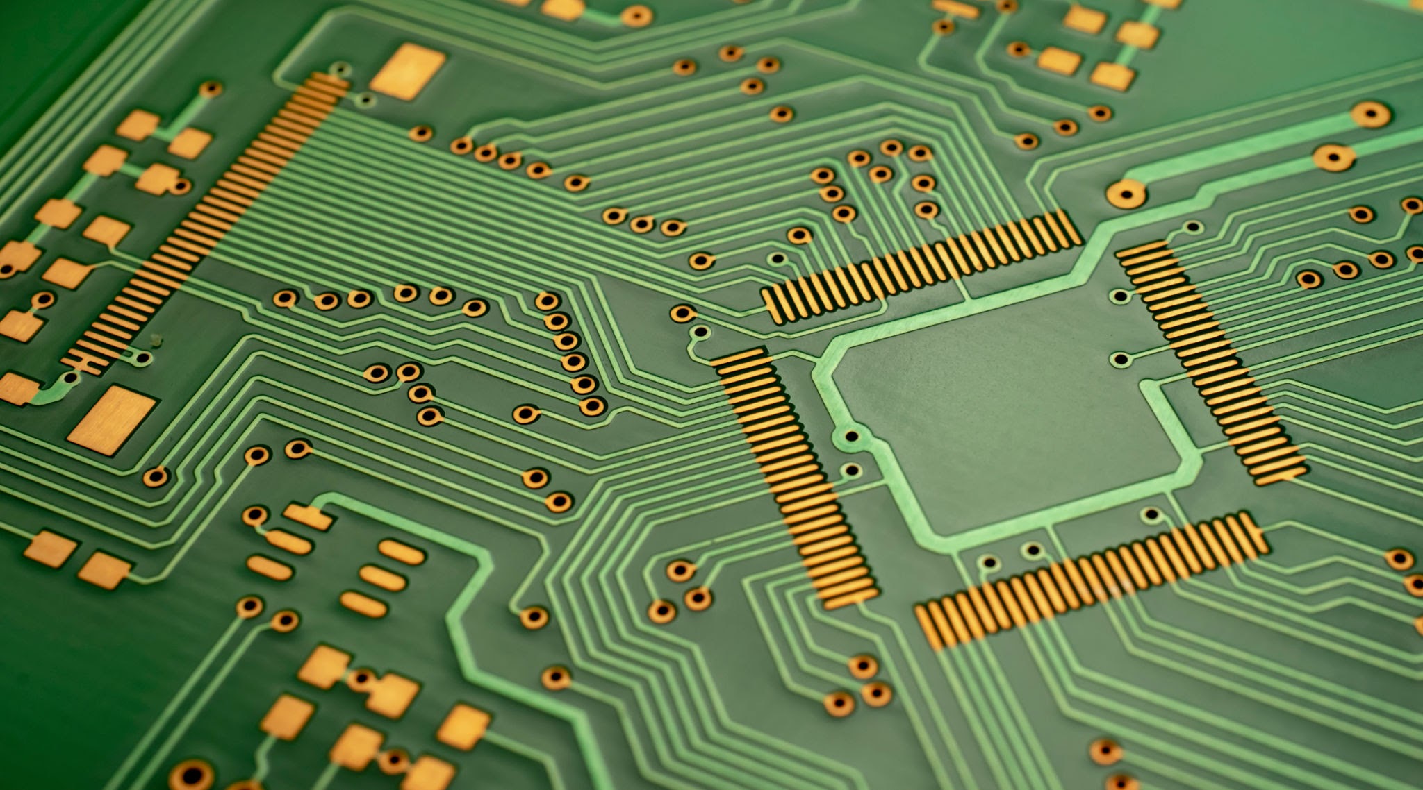
The folding PCBs (Flexible Printed Circuit Boards, FPCBs) in foldable devices involve chemical etching to create fine conductive traces on thin copper or other conductive materials. Here’s what’s involved:
- Materials Involved: Flexible substrates such as polyimide (PI) or PET (polyethylene terephthalate), with copper or other metal layers used for the conductive pathways.
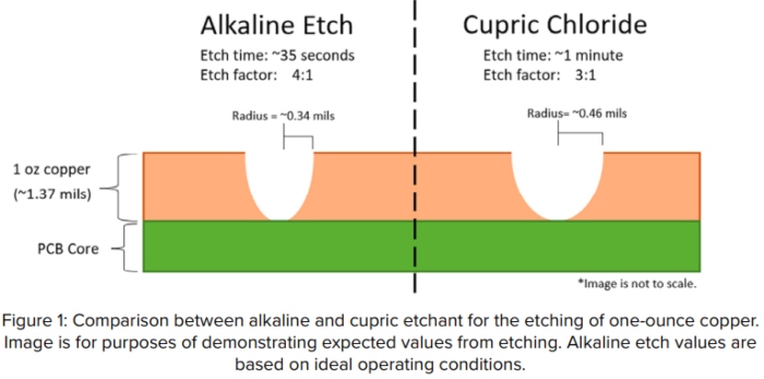
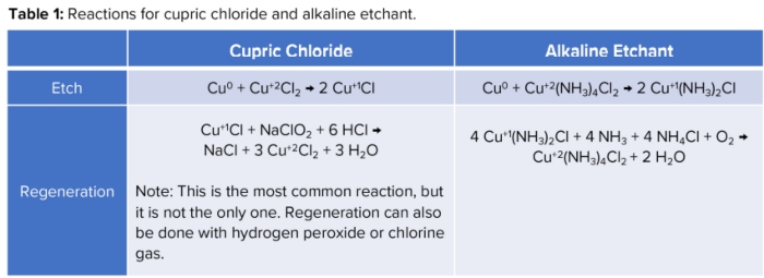
- Etching Process: The primary method is chemical etching for subtractive manufacturing, where unwanted copper is removed to leave behind the desired circuit pattern. This is done using acidic solutions (like ferric chloride or cupric chloride).
- Equipment:
- Roll-to-roll etching machines: These are commonly used in high-volume production for flexible circuits. They are designed to handle continuous sheets of substrate material, enabling efficient large-scale production.
- Precision etching machines: These machines are capable of producing fine lines and intricate patterns required for folding PCBs, ensuring flexibility and durability without compromising electrical performance.
Additional Considerations
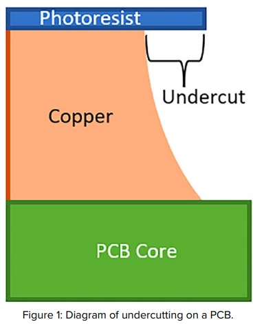
- Masking Process: Both the screen and PCB require photoresist application and development to mask areas that should not be etched. This is commonly done with photoresist coating machines and UV exposure systems.
- Cleanroom Environment: Due to the precision required, these processes take place in a cleanroom environment to avoid contamination, especially for display components.
- Etching Control: Real-time monitoring and control systems are critical to ensure etch depth uniformity, particularly for thin and flexible materials.
By using a combination of chemical etching and advanced processing equipment, manufacturers can create the fine, flexible structures required for both the screen and folding PCBs in devices like the Huawei Mate XT.

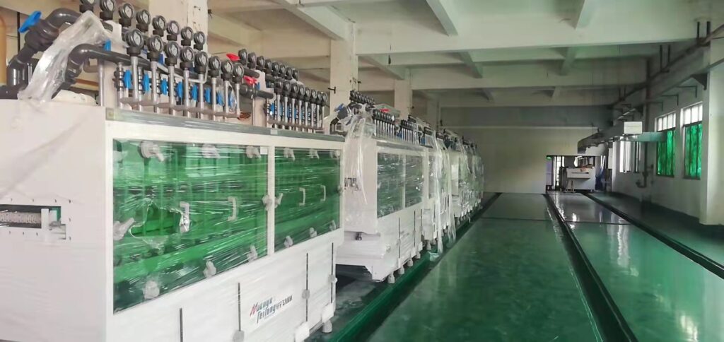
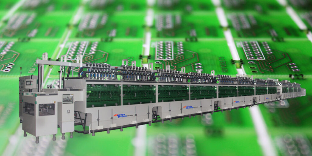
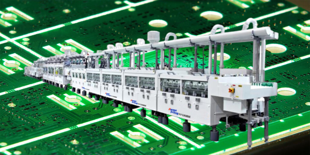
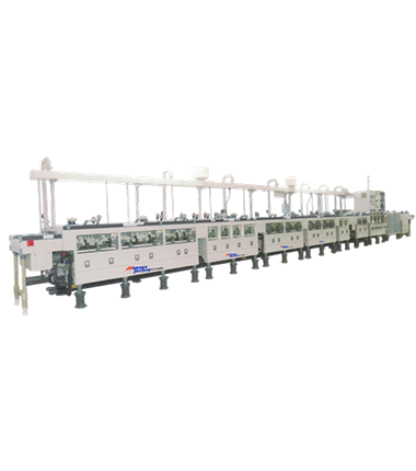
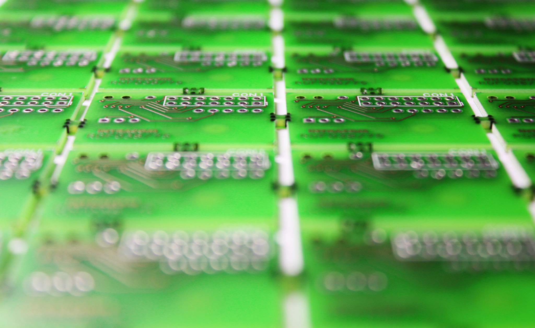
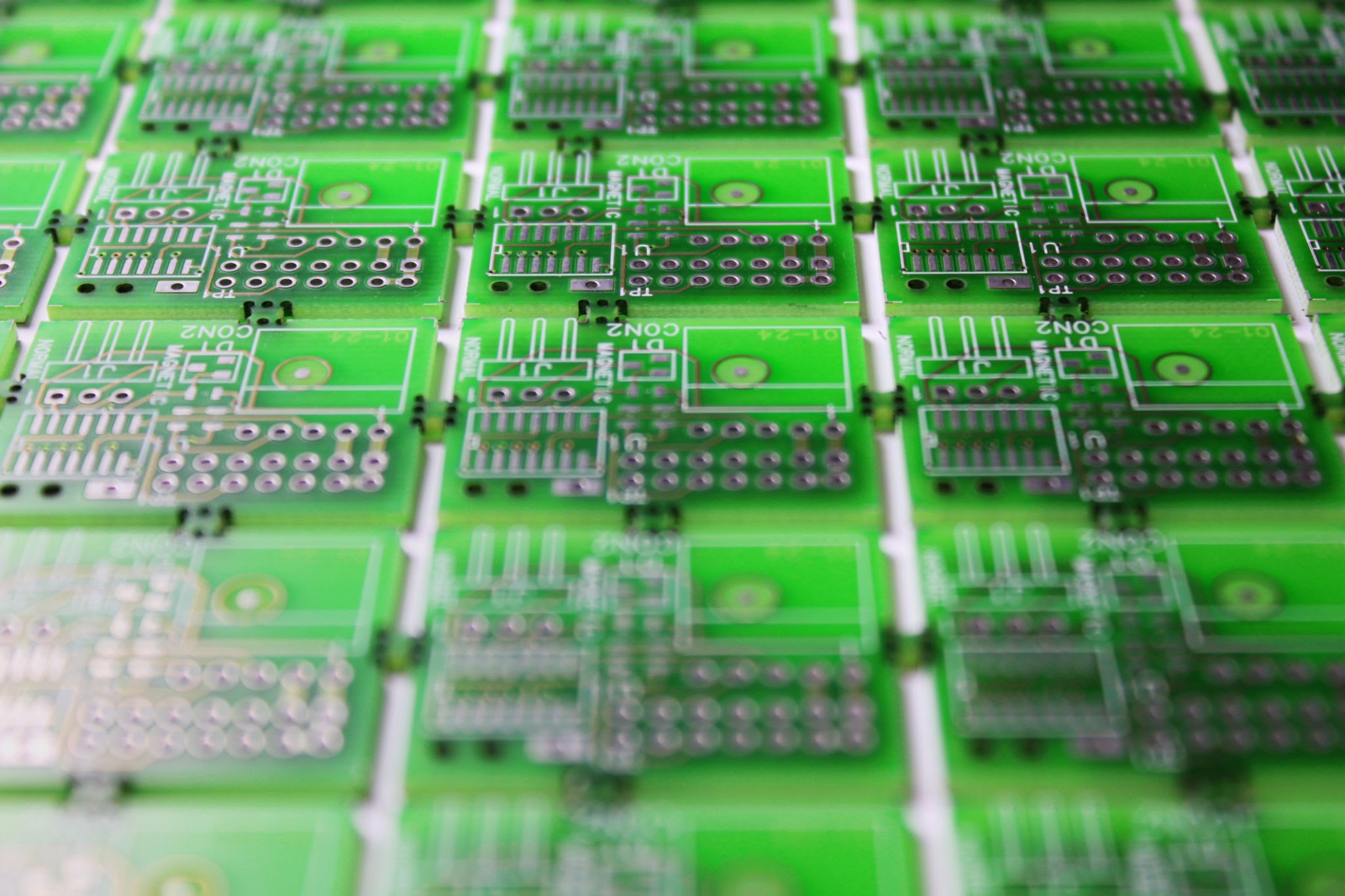
Here’s a comprehensive list of the chemical processing equipment typically involved in the production of flexible PCBs (FPCBs), along with the corresponding steps:
1. Material Preparation
- Laminators: Used to apply the copper-clad film onto the flexible substrate (e.g., polyimide or PET).
2. Photoresist Application
- Coaters: Machines for applying a layer of photoresist (dry film or liquid photoresist) on the copper surface. This is critical for defining the circuit pattern during the etching process.
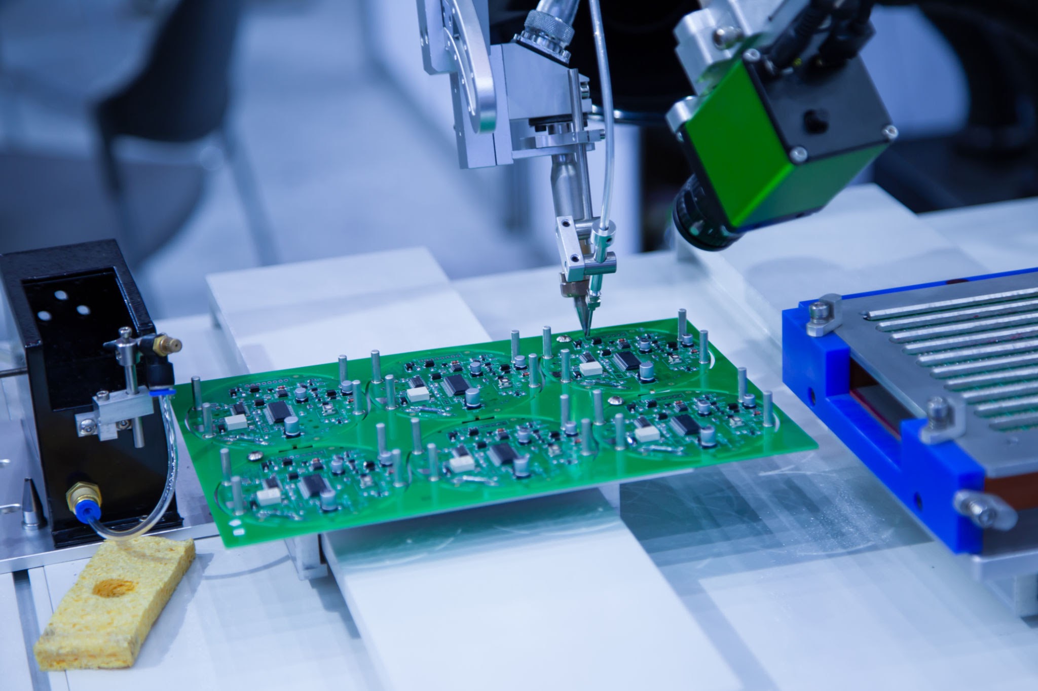
3. Laser Direct Imaging (LDI) Exposure
- LDI Exposure Machines: These systems expose the photoresist layer to UV light in the exact circuit pattern based on CAD files. LDI ensures high precision, especially for the fine lines needed in flexible PCBs.
4. Development Process
- Developers: Once the photoresist is exposed, developers are used to wash away the unexposed areas of the photoresist, leaving only the areas that will protect the copper during etching. Alkaline solutions are commonly used for this process.
5. Etching Process
- Chemical Etching Machines: These remove the unmasked copper to form the circuit traces. Ferric chloride or cupric chloride is used for copper etching. For flexible PCBs, this equipment is often in a roll-to-roll configuration to handle continuous substrates efficiently.
6. Stripping Process
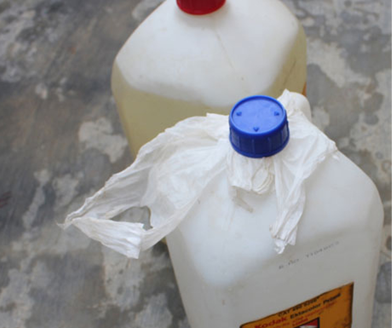
- Strippers: After etching, the remaining photoresist (which protected the copper traces) needs to be removed. Strippers use chemical solutions like alkaline-based chemicals to strip the photoresist.
7. Cleaning and Drying
- Cleaning Machines: The FPCB needs thorough cleaning to remove residues from the etching and stripping processes. Cleaning machines use deionized water or other specialized cleaning agents.
- Dryers: High-precision drying equipment is used to completely dry the flexible PCBs to avoid defects caused by residual moisture.
8. Solder Mask Application (Optional)
- Coaters: A solder mask can be applied to protect the copper traces except for areas where components will be soldered. This is done using spray coating or screen printing.
- LDI Machines: Similar to earlier, LDI exposure machines may be used to precisely define the areas where the solder mask should be removed.
9. Post-Processing
- Surface Treatment: Flexible PCBs often undergo surface treatments like electroless nickel immersion gold (ENIG) or OSP (organic solderability preservative) to enhance solderability and prevent oxidation.
- Cutting/Profiling: Finally, the flexible PCBs may need to be cut into specific shapes using laser cutters or CNC routers.
10. Testing
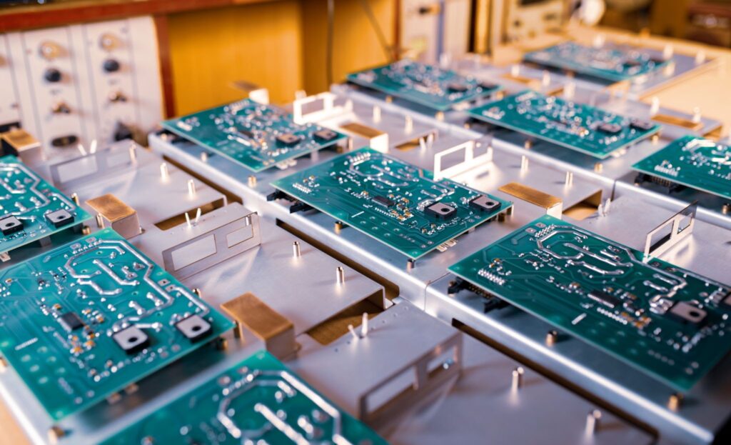
- Automated Optical Inspection (AOI): This machine scans the finished flexible PCB to check for defects like open circuits or short circuits.
- Electrical Testing Equipment: To verify the electrical properties of the circuits, ensuring functionality.
Summary of Equipment:
- Laminators (for applying copper-clad film)
- Photoresist Coaters (dry film or liquid)
- LDI Exposure Machines (for circuit pattern imaging)
- Chemical developing machine (to remove unexposed photoresist)
- Chemical Etching Machines (ferric or cupric chloride)
- Chemical Stripper Machine (for removing remaining photoresist)
- Chemical Cleaning Machines (for post-etching and stripping)
- Dryers (to eliminate moisture)
- Coaters and LDI for Solder Mask (optional)
- Surface Treatment Equipment (for solderability)
- Cutting Machines (laser or CNC for profiling)
- AOI and Electrical Testing Machines (for inspection)
These steps ensure that the flexible PCB is precisely etched, cleaned, and ready for further assembly into complex devices like Huawei’s foldable Mate XT.