All posts by droganetching

Revolutionizing PCB Manufacturing: How MacroFab’s Innovative Approach and Advanced Technology are Changing the Game

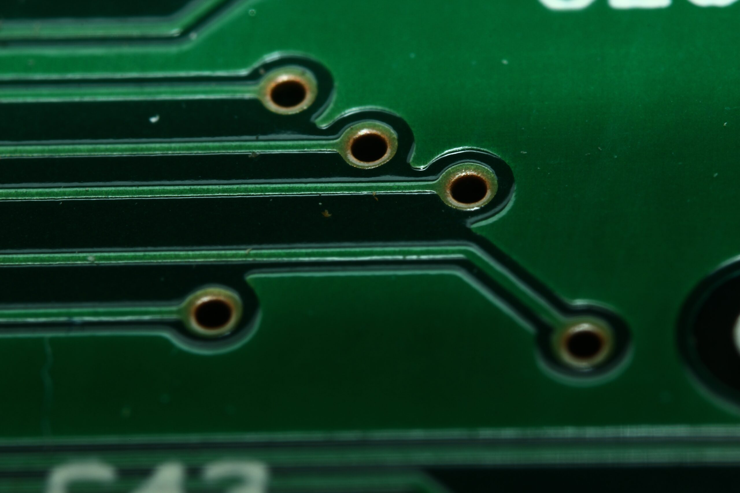
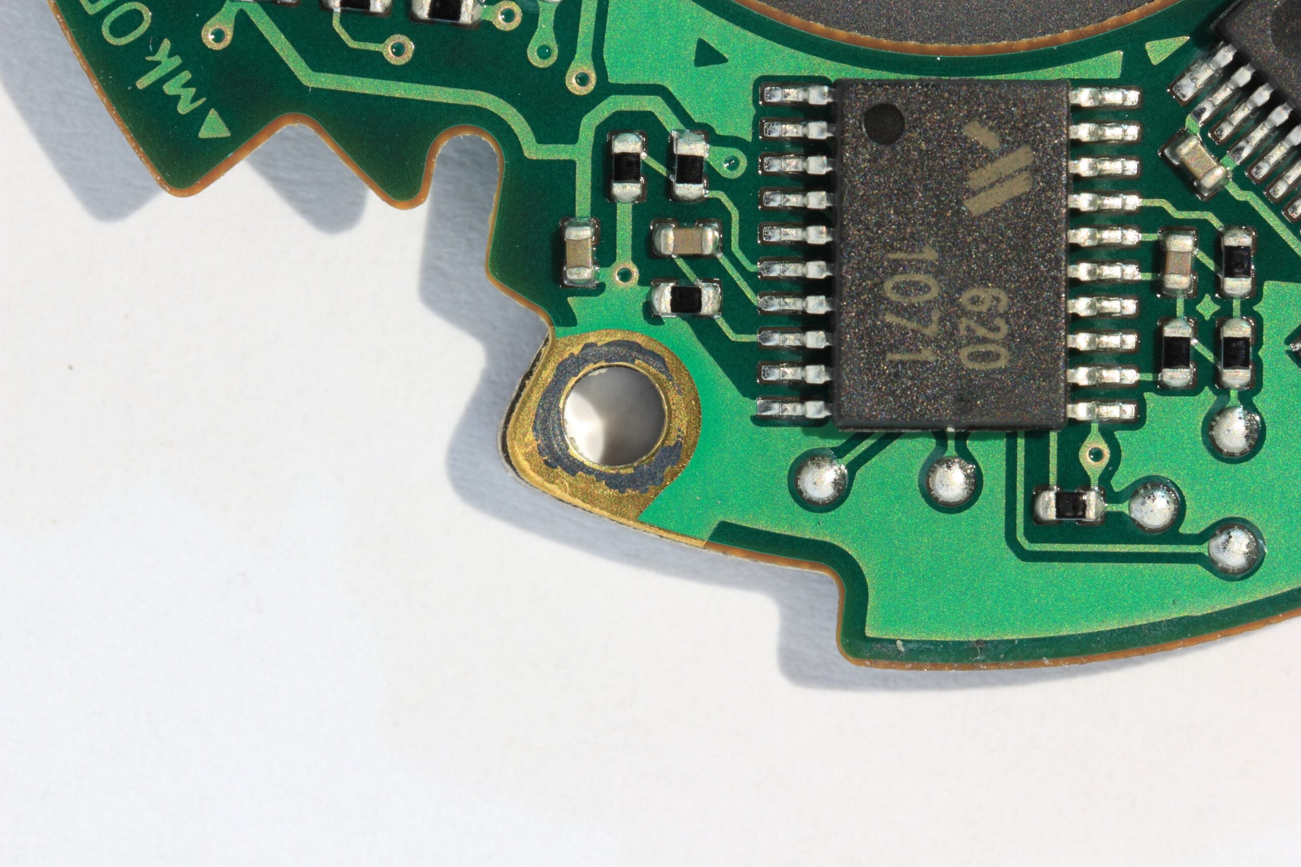
Printed Circuit Board (PCB) manufacturing has become an essential part of the manufacturing industry as electronic devices continue to proliferate. In recent years, the digital transformation of the manufacturing industry has brought significant opportunities and challenges to the PCB manufacturing sector. MacroFab, a company that specializes in PCB assembly, is at the forefront of this transformation, providing cutting-edge solutions to meet the growing demands of the industry.

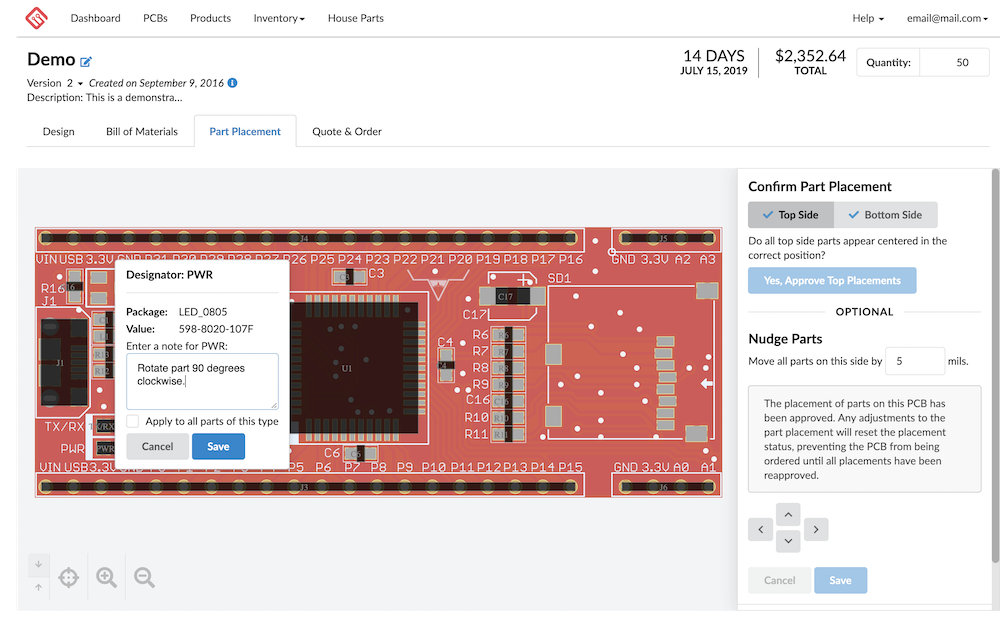
MacroFab’s innovative approach to PCB assembly includes the use of automated assembly lines, advanced software, and machine learning algorithms. These technologies allow the company to produce high-quality PCBs with greater efficiency and precision than traditional manufacturing methods. The automated assembly lines, for example, can handle high volumes of PCBs with minimal human intervention, reducing the likelihood of errors and increasing production speed.

The use of advanced software and machine learning algorithms also allows MacroFab to optimize its manufacturing processes. By analyzing data on production processes and identifying areas of inefficiency, the company can improve its operations and reduce costs. This, in turn, allows MacroFab to offer its customers competitive pricing while maintaining high-quality standards.

Another advantage of MacroFab’s approach to PCB assembly is its ability to customize its solutions to meet the specific needs of its customers. Whether it’s a small-scale project or a large-scale production run, MacroFab can tailor its services to meet the unique requirements of each customer. This flexibility is essential in today’s fast-paced manufacturing industry, where agility and responsiveness are crucial for success.

In conclusion, the digital transformation of the manufacturing industry has brought significant changes to the PCB manufacturing sector, and companies like MacroFab are leading the way in this transformation. With their innovative approach to PCB assembly, advanced technologies, and customer-centric approach, MacroFab is well-positioned to meet the growing demands of the industry and help shape its future.

As a manufacturer of PCB etching machines, you understand the critical role that this equipment plays in the manufacturing process. With the increasing demand for electronic devices, the need for high-quality PCBs has never been greater. MacroFab, a leading company in the PCB assembly industry, has demonstrated how innovative solutions and advanced technology can meet this demand while providing cost-effective solutions for its customers.

MacroFab’s use of automated assembly lines, advanced software, and machine learning algorithms has revolutionized the PCB assembly process. By automating the assembly process, MacroFab can handle high volumes of PCBs with minimal human intervention, reducing the risk of errors and increasing production speed. The use of advanced software and machine learning algorithms allows MacroFab to optimize its manufacturing processes by analyzing data and identifying areas of inefficiency.

The company’s customer-centric approach allows it to customize its services to meet the specific needs of each customer, from small-scale projects to large-scale production runs. This flexibility is crucial in today’s fast-paced manufacturing industry, where agility and responsiveness are essential for success.

As a PCB etching machine manufacturer, you can learn from MacroFab’s success and apply their principles to your business. By investing in innovative solutions and advanced technology, you can improve the efficiency and precision of your machines, providing cost-effective solutions for your customers. Additionally, you can adopt a customer-centric approach, providing customized services that meet the unique needs of your customers.

In conclusion, the case of MacroFab’s success in the PCB assembly industry provides valuable lessons for PCB etching machine manufacturers. By investing in innovation and advanced technology and adopting a customer-centric approach, you can differentiate your business and provide high-quality, cost-effective solutions for your customers. As the demand for electronic devices continues to grow, it’s essential to position yourself as a leader in the industry, providing solutions that meet the needs of your customers and help shape the future of PCB manufacturing.

Conclusion: The digital transformation of the manufacturing industry has brought significant changes to the PCB manufacturing sector. The success of MacroFab in the PCB assembly industry provides valuable lessons for PCB etching machine manufacturers. By embracing innovation and a customer-centric approach, manufacturers can differentiate themselves and provide high-quality, cost-effective solutions for their customers. As the demand for electronic devices continues to grow, it is essential to position oneself as a leader in the industry, providing solutions that meet the needs of customers and help shape the future of PCB manufacturing.

The Impact of Artificial Intelligence (Ai) on the PCB Industry

Artificial intelligence (AI) is revolutionizing the way printed circuit boards (PCBs) are designed, manufactured, and tested. AI algorithms are optimizing PCB layouts, reducing defects, and predicting equipment failures. Discover how AI is transforming the PCB industry and what the future may hold.

Artificial intelligence (AI) has the potential to revolutionize many industries, and the printed circuit board (PCB) industry is no exception. In fact, AI is already having a significant impact on the way PCBs are designed, manufactured, and tested.

Design: One of the main ways AI is impacting the PCB industry is through the design process. Designers can use AI algorithms to optimize the layout of a PCB, minimizing the number of components needed and reducing signal interference. This results in more efficient and reliable PCBs, with fewer errors and better performance.

Manufacturing: AI is also being used to improve the manufacturing process of PCBs. Automated optical inspection (AOI) systems use machine learning algorithms to detect and classify defects in PCBs. This allows for more accurate and efficient inspections, reducing the number of defective PCBs produced.

Furthermore, AI can help to optimize the manufacturing process by predicting and preventing equipment failures. Machine learning algorithms can analyze data from sensors in production equipment to detect anomalies and predict when equipment is likely to fail. This allows for preventative maintenance to be performed, reducing downtime and increasing efficiency.

Testing: AI can also improve the testing process for PCBs. Automated testing systems can use machine learning algorithms to detect and classify defects in PCBs during the testing process. This reduces the time and cost associated with manual testing, while also improving the accuracy of the testing process.

Future of AI in PCB industry: As AI technology continues to evolve, the impact on the PCB industry is likely to grow. One potential area of development is in the use of AI to improve the supply chain. Machine learning algorithms can analyze data on component availability, lead times, and pricing to optimize the supply chain and reduce costs.

Another potential development is in the use of AI to optimize the thermal management of PCBs. Machine learning algorithms can analyze thermal data from PCBs to optimize the layout and component placement, reducing the risk of overheating and improving the reliability of the PCB.

Conclusion: AI is already having a significant impact on the PCB industry, improving the design, manufacturing, and testing processes. As the technology continues to evolve, the potential for further improvements is vast. The use of AI to optimize the supply chain and thermal management of PCBs are just two potential areas of development. It is clear that AI is set to play a major role in the future of the PCB industry.

What to Make of U.S. Government Will Support Domestic PCB Manufacturing

The United States government is taking initiatives to support domestic manufacturing of printed circuit boards (PCBs). The move is aimed at promoting technological self-sufficiency and reducing dependence on foreign manufacturing. This report will discuss the challenges faced by the domestic PCB manufacturing industry and the government’s efforts to support it.

U.S. Government Will Support Domestic PCB Manufacturing

Challenges faced by domestic PCB manufacturing industry: The domestic PCB manufacturing industry has faced several challenges in recent years, including competition from cheaper imports, lack of investment in research and development, and the high cost of manufacturing equipment. This has resulted in a decline in the number of domestic PCB manufacturers and a growing dependence on foreign manufacturers.

Government’s initiatives to support domestic PCB manufacturing: The U.S. government has announced several initiatives to support domestic PCB manufacturing. One such initiative is the creation of a public-private partnership called the American Institute for Manufacturing of Advanced PCBs (AIM Photonics). This partnership aims to provide funding for research and development of advanced technologies, such as high-density interconnect (HDI) PCBs, which are commonly used in advanced packaging applications.

The government has also announced a plan to provide financial incentives for domestic PCB manufacturers to invest in new equipment and technology. The incentives are expected to make it easier for domestic manufacturers to purchase new equipment and upgrade their facilities, thus making them more competitive in the global market.

Additionally, the government plans to establish a network of advanced manufacturing institutes across the country that will focus on developing and implementing advanced manufacturing technologies, including PCB manufacturing. These institutes will provide technical support and training to domestic manufacturers, enabling them to develop and adopt new manufacturing techniques and technologies.

Conclusion: The government’s efforts to support domestic PCB manufacturing are a welcome move that will help promote technological self-sufficiency and reduce dependence on foreign manufacturers. By providing funding for research and development of advanced technologies and financial incentives for domestic manufacturers, the government is helping to create a more competitive domestic PCB manufacturing industry. The establishment of advanced manufacturing institutes across the country will also provide technical support and training to domestic manufacturers, helping them to stay up-to-date with the latest manufacturing techniques and technologies.

What technical support is required for packaging PCB?

To package PCBs, a variety of technical support is required, including:

  • Design software: Packaging PCBs requires specialized design software that can create and test the packaging design before it goes into production. This software must be able to create 3D models of the PCB, generate the necessary manufacturing files, and perform simulations to ensure the design meets the required specifications.
  • Manufacturing equipment: Once the PCB packaging design is finalized, it needs to be manufactured. This requires specialized equipment, such as pick-and-place machines, soldering equipment, and testing equipment, to assemble the PCB components and test the final product.
  • Material selection: Selecting the right materials is critical to ensuring the PCB packaging meets the required specifications. Technical support is required to help choose the right materials based on factors such as the operating environment, durability, and electrical properties.
  • Thermal management: PCBs generate heat, and packaging design needs to include thermal management strategies to ensure the PCB doesn’t overheat. Technical support is required to help determine the best thermal management strategy, including heat sinks, fans, and other cooling methods.
  • Compliance testing: The PCB packaging design needs to meet various regulatory requirements and industry standards. Technical support is required to ensure the design meets these standards and passes compliance testing.

Overall, packaging PCBs requires a significant amount of technical expertise and support to ensure the final product meets the required specifications and performs as intended.

PCB Production Process: A Complete Guide to Designing and Manufacturing Machines Electronic Circuits

Printed Circuit Boards (PCBs) are an essential component of modern electronic devices. PCBs provide a means of interconnecting electronic components, enabling the creation of complex and sophisticated electronic systems. The production of PCBs involves a series of steps that require precision, expertise, and specialized equipment. In this blog post, we will discuss the PCB production process in detail.

PCB Design:

The first step in the production of PCBs is the design phase. During this phase, engineers use computer-aided design (CAD) software to create a schematic diagram and a physical layout of the circuit. The circuit layout is the blueprint for the final product, and it determines the placement of electronic components and the routing of electrical connections.

PCB Manufacturing:

Once the circuit layout is finalized, the PCB manufacturing process can begin. The circuit layout is printed on a copper-clad board using a process called etching. The board is coated with a layer of photoresist, which is then exposed to UV light through a stencil of the circuit layout. The unexposed areas of the photoresist are then dissolved, leaving behind a pattern of copper on the board. This pattern of copper traces makes up the circuit.

Dragon Etching: Inside Look at PCB Manufacturing,test, from Workshop to Shipping | Sunset Delivery
PCB etching machine plants

PCB Etching:

Etching is the process of removing unwanted copper from the PCB to create the desired circuit pattern. It is done by exposing the board to an etchant, which selectively removes the copper from the areas not protected by the photoresist. After the etching process is complete, the remaining photoresist is stripped away, leaving behind the desired circuit pattern.

Home
PCB Etching Machine

PCB Developing Exposing:

The board is then developed using a chemical solution that dissolves the exposed photoresist, leaving behind the copper pattern that makes up the circuit. This process is known as developing.

Home
PCB Developing Exposing Machine

PCB Stripping:

Once the copper pattern is developed, the remaining photoresist must be stripped away using a chemical solution, leaving only the copper traces behind. This process is known as stripping.

Home
PCB Stripping Machine

PCB Cleaning:

After stripping, the board is thoroughly cleaned to remove any chemical residue and ensure a clean surface for the next step.

Home
PCB Cleaning Machine

PCB Desoldering:

During the assembly process, electronic components may need to be removed or replaced, requiring desoldering. This is done using specialized tools and techniques to remove the solder holding the component in place without damaging the board or the component.

Home
PCB Desoldering Machine

PCB Oxidation Resistance:

PCBs are susceptible to oxidation, which can cause corrosion and damage to the board over time. To prevent this, a layer of oxidation-resistant material is applied to the board to protect it from the environment.

Home
PCB Oxidation Resistance Machine

PCB Polishing:

Home
PCB Polishing Machine

After the oxidation-resistant layer is applied, the board may be polished to create a smooth surface and ensure the proper thickness of the copper traces.

PCB Sandblasting:

In some cases, the board may be sandblasted to create a rough surface for improved adhesion of the oxidation-resistant material.

Home
PCB Sandblasting Machine

PCB Browning:

Finally, the board may be treated with a chemical solution to create a brown or black surface that provides a contrast for easier inspection and testing.

In conclusion, the production of PCBs involves a series of steps that require precision, expertise, and specialized equipment. The PCB production process is critical to the functioning and performance of electronic devices, and it must be executed with care and attention to detail.

Home
PCB Browning Machine