As technology advances, so does our demand for smaller and more intricate electronic devices. Behind these cutting-edge gadgets lies the fascinating world of printed circuit boards (PCBs). Within PCB fabrication, the use of alkaline etchants has revolutionized the process of wet etching. In this blog, we will explore the ins and outs of alkaline etchants, uncovering the technique’s details for employing them in PCB wet etching machines.
What is Alkaline Etchant?
Alkaline etchant is a potent chemical solution utilized in the PCB manufacturing process. Composed mainly of alkaline substances such as sodium hydroxide (NaOH) or potassium hydroxide (KOH), this etchant is specially designed to selectively remove copper or other metallic materials from the PCB substrate. The purpose of this precise removal is to create specific circuit patterns and interconnections on the board.
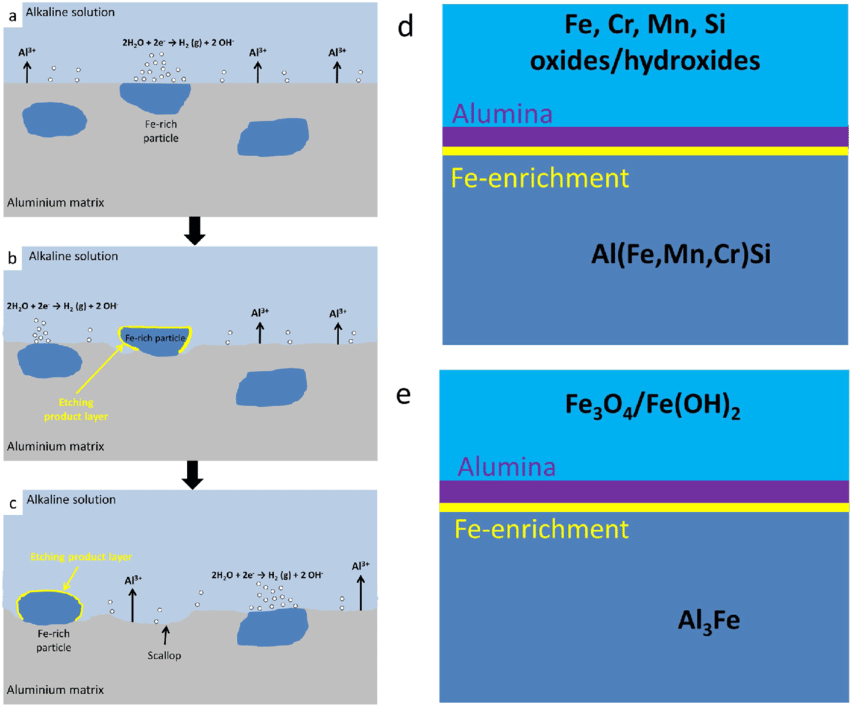
Schematic diagrams illustrating the progressive alkaline etching process Image from:https://www.researchgate.net/figure/Schematic-diagrams-illustrating-the-progressive-alkaline-etching-process-a-c-and-the_fig11_346886096
The Technique of Using Alkaline Etchant for PCB Wet Etching Machine:
Preparing the PCB:
Before delving into the wet etching process, it is essential to ensure that the PCB is thoroughly cleaned and dried. Any contaminants or residues must be removed to guarantee optimal etching results.
Etchant Composition:
Creating the right alkaline etchant solution is crucial for the success of the wet etching process. The proper concentration of the alkaline substance and any additional additives must be meticulously calculated and mixed. These additives may include stabilizers to control etch rates or improve solution stability.
Immersion in Alkaline Etchant:
Once the etchant solution is prepared, the PCB is carefully immersed in the solution. For large-scale PCB manufacturing, automated wet etching machines are employed to ensure consistent and uniform etching across the substrate.
Time and Temperature Control:
The key to achieving precise circuit patterns lies in controlling the etching time and temperature. The duration of immersion and the temperature of the etchant solution must be meticulously regulated to prevent over-etching or under-etching, both of which can lead to defective PCBs.
Agitation:
In some cases, gentle agitation of the etchant solution is used to enhance the etching process further. Proper agitation ensures the even distribution of the etchant across the PCB surface, leading to uniform results.
Rinse and Neutralization:
After the etching process is complete, the PCB is thoroughly rinsed with water to remove any remaining etchant solution. Additionally, the PCB may undergo a neutralization step to ensure the complete deactivation of the etchant.
Alkaline etchant has proven to be a game-changer in the world of PCB wet etching. By harnessing the power of this precise chemical solution, PCB manufacturers can create intricate circuit patterns, essential for modern electronic devices. Understanding the technique of using alkaline etchant, from its preparation to its application in wet etching machines, empowers engineers to deliver high-quality, reliable, and innovative PCBs for a myriad of technological applications.
Embrace the magic of alkaline etchant and dive into the realm of endless possibilities in PCB fabrication!
The semiconductor wet process, also known as wet etching or wet cleaning, refers to a set of techniques used in semiconductor manufacturing to modify or clean the surfaces of semiconductor materials using liquid chemicals. It involves the controlled application of specific chemical solutions onto the surface of a semiconductor wafer to achieve various purposes, such as etching, cleaning, or surface preparation.
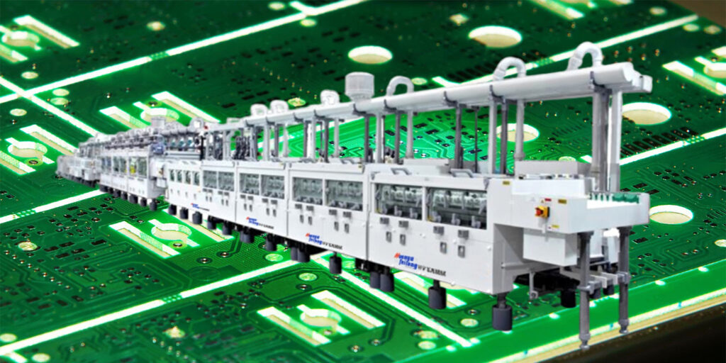
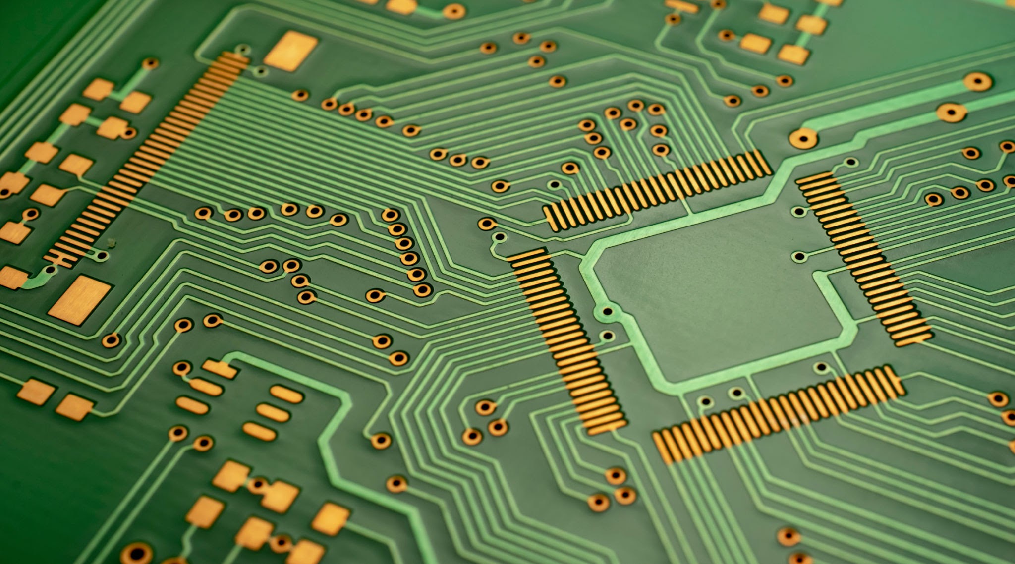
Chemical etching machine
Wet etching is primarily used for selective removal of material layers from the surface of a semiconductor wafer. This process involves immersing the wafer into a liquid etchant, such as an acid or a base, that selectively reacts with the target material, dissolving it and leaving the desired pattern or structure intact. Wet etching is commonly used for creating patterns, such as trenches, wells, or isolation regions, in integrated circuits.
How much does t cost to produce PCB
Design complexity: The more complex the design, with intricate circuitry, smaller trace widths, and finer pitch components, the higher the manufacturing cost. Complex designs may require advanced fabrication techniques or specialized equipment.
Number of layers: PCBs can have single-layer, double-layer, or multilayer designs. Multilayer PCBs typically have higher manufacturing costs due to the additional layers and increased complexity in fabrication.
Quantity: PCB manufacturers often offer volume discounts, meaning that producing a higher quantity of PCBs can reduce the cost per unit. However, prototyping or low-volume production may have higher per-unit costs.
Materials: The choice of materials can impact the cost. High-quality materials or specialized laminates can be more expensive. Additionally, if specific materials are required for specialized applications or high-frequency designs, the cost may increase.
Manufacturing options: Various manufacturing options, such as surface mount technology (SMT) assembly, through-hole assembly, or specialized processes like gold plating, can affect the cost. Additional processes like solder mask application, silkscreen printing, or panelization can also contribute to the overall cost.
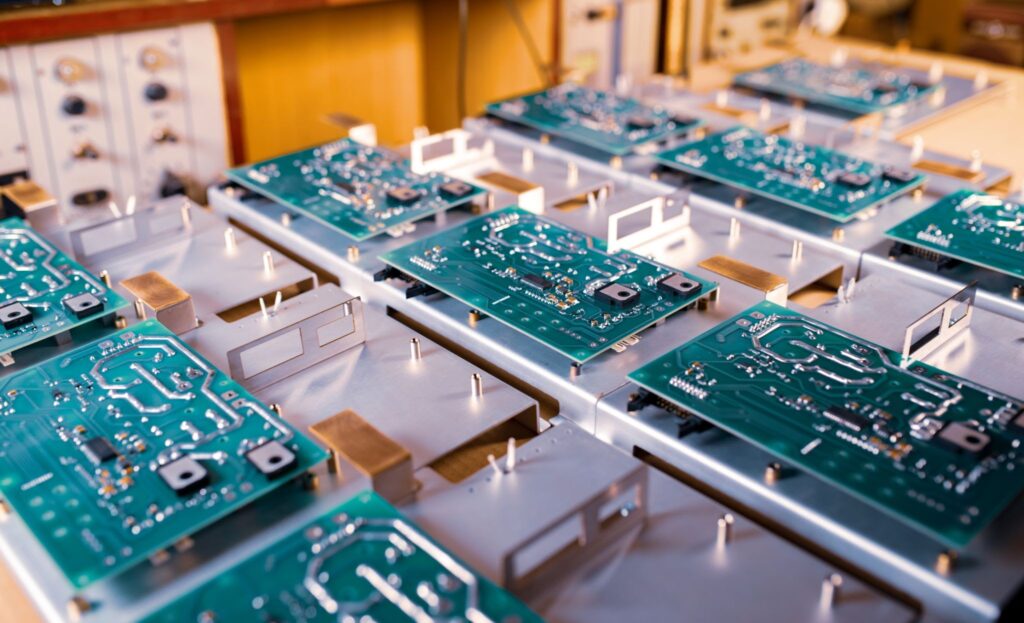
Shot of an Electronics Factory Workers Assembling Circuit Boards by Hand While it Stands on the Assembly Line. High Tech Factory Facility.
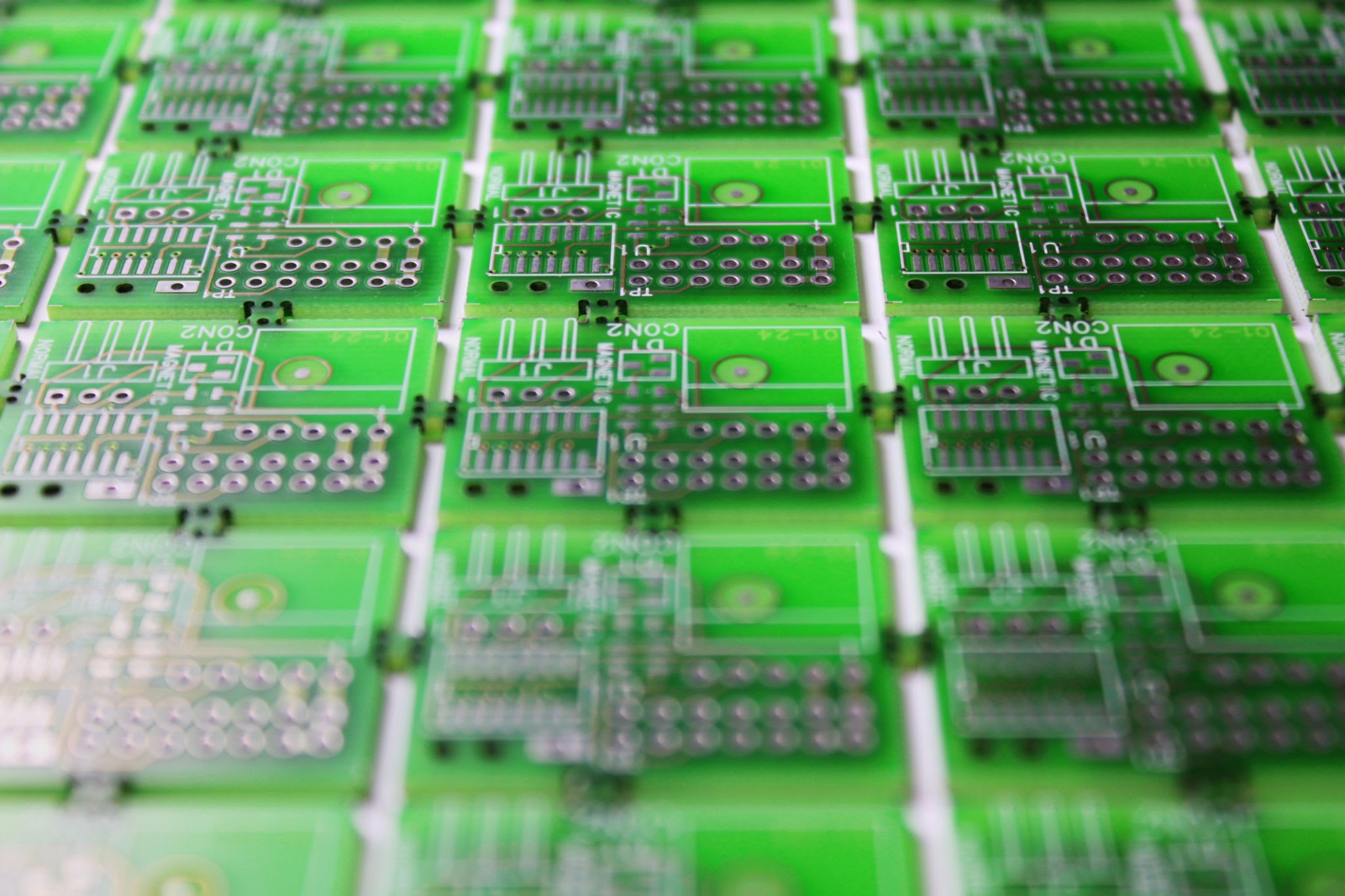
Semiconductor(PCB) wet process equipment
Etching Machine: These machines are used for the chemical etching process to remove unwanted copper from the PCB surface. Spray etching machines, dip tanks, and conveyorized spray etching systems are commonly used for this purpose.
Developing Machine: Developing machines are used during the photoresist imaging process. They apply developer chemicals to remove the unexposed photoresist, revealing the desired circuit pattern.
Stripping Machine: Stripping machines are used to remove the remaining photoresist or solder mask after the etching process. They employ stripping chemicals to dissolve and clean the surface.
Plating Machine: Plating machines are utilized for the electroplating process to deposit a layer of metal, such as copper or gold, onto the PCB. These machines ensure controlled and uniform plating to create circuit traces or enhance conductivity.
Cleaning Machine: Cleaning machines are used for various cleaning steps throughout the PCB manufacturing process. They employ cleaning solutions to remove contaminants, residues, and particles from the PCB surface.
Rinse Machine: Rinse machines are employed to rinse the PCBs after each wet processing step to remove any remaining chemicals or contaminants. They typically use deionized water or other rinsing agents.
Difference between dry process and wet process
The main difference between dry process and wet process lies in the state of the materials or substances involved and the nature of the processes used. Here’s a general overview of the differences:
Dry Process:
State of Materials: In a dry process, the materials involved are typically in a solid or gaseous state, with little or no involvement of liquid substances.
Lack of Liquid Media: Dry processes generally do not involve the use of liquid media or solvents.
Examples of Dry Processes: Dry processes can include techniques like dry etching (such as plasma etching or reactive ion etching), physical vapor deposition (PVD), dry cleaning, or dry surface treatment. These processes often rely on gas-phase reactions or physical mechanisms.
Advantages: Dry processes can offer precise control, high resolution, and selectivity. They are often faster, more environmentally friendly, and can be more suitable for delicate or sensitive materials that may be affected by liquid exposure.
Disadvantages: Dry processes may have limitations in terms of uniformity, compatibility with certain materials or substrates, and may require more specialized equipment.
Wet Process:
State of Materials: Wet processes involve the use of liquid chemicals or solutions as a medium to carry out the desired reactions or treatments.
Involvement of Liquid Media: Wet processes rely on immersing or applying liquid media to the materials being processed.
Examples of Wet Processes: Wet processes can include wet etching, wet cleaning, chemical vapor deposition (CVD), electroplating, or wet surface treatment. These processes often involve chemical reactions and interactions between the materials and the liquid media.
Advantages: Wet processes can offer excellent selectivity, high throughput, and good coverage over large areas. They are commonly used for bulk material removal, cleaning, and deposition of thin films.
Disadvantages: Wet processes may require careful handling of hazardous chemicals, can introduce contaminants or require additional rinsing steps, and may have limitations in achieving high aspect ratios or sharp features.
Both dry and wet processes have their own advantages and are employed in various industries and applications. The choice between the two depends on factors such as the desired outcome, material compatibility, process requirements, and the specific manufacturing or treatment objectives.
Why wet process is important?
The wet process is important for several reasons, especially in the context of semiconductor manufacturing and other industries that involve precise material modification and cleaning. Some of the key reasons why the wet process is important include:
Selective Material Removal: Wet etching is a crucial technique for selectively removing specific materials from the surface of semiconductor wafers or other substrates. This allows for the creation of intricate patterns, trenches, and isolation regions required for integrated circuits and microelectronics.
Precision Surface Cleaning: Wet cleaning is essential for removing impurities, particles, and organic residues from the surface of wafers and other components. Clean surfaces are vital for ensuring the reliability and performance of semiconductor devices and other precision electronics.
Compatibility with Delicate Materials: Wet processes are often more compatible with delicate or sensitive materials, as they do not subject the materials to high temperatures or harsh mechanical forces like some dry processes might. This is especially crucial in semiconductor manufacturing, where certain materials can be damaged or altered by dry processes.
High Throughput: Wet processes can achieve high throughput, making them suitable for large-scale production in semiconductor fabrication facilities or other industries requiring mass production.
Contamination Control: Wet processes can be designed to minimize contamination issues by using carefully controlled chemicals and rinsing steps, ensuring the purity of the final product.
Low Cost: In some cases, wet processes can be more cost-effective than dry processes, especially when dealing with high-volume production.
Uniformity: Wet processes can provide uniform deposition, etching, or cleaning over large areas, making them suitable for applications requiring consistent results across a substrate.
Customization: The wet process can be tailored to specific requirements by adjusting chemical concentrations, process times, and temperature, enabling a wide range of applications and desired outcomes.
Due to these advantages, the wet process remains an integral part of semiconductor manufacturing, microelectronics, photovoltaic cell production, and various other industries requiring precise material modification and cleaning. While dry processes offer their own benefits, wet processes play a vital role in achieving the required levels of precision, uniformity, and compatibility with a diverse range of materials and applications.
Frequency converters, also known as power converters or frequency changers, are electronic devices used to convert electrical power from one frequency to another. The composition of a frequency converter can vary depending on its specific application and power rating. However, here are the common components found in frequency converters:
Rectifier: The rectifier is responsible for converting the incoming alternating current (AC) power into direct current (DC) power. It typically consists of diodes arranged in a bridge configuration to rectify the AC waveform.
Diodes: Rectifiers use semiconductor diodes, typically in a bridge configuration, to convert AC power to DC power. Diodes are made up of semiconductor materials, such as silicon or germanium, with a p-n junction that allows current flow in one direction while blocking it in the reverse direction.
Heat sinks: Since rectifiers can generate heat during operation, heat sinks are often attached to diodes to dissipate heat and prevent damage to the components. Heat sinks are made of thermally conductive materials, such as aluminum or copper, with fins to increase the surface area for efficient heat dissipation.
How are the Diodes, Heat sinks inside the Rectifier of Frequency Converters made?
DC Link: The DC link is a capacitor bank or an energy storage device that smoothens the rectified DC voltage and provides a stable DC voltage source to the inverter.
Capacitors: The DC link uses capacitors to store electrical energy and provide a stable DC voltage source to the inverter. Electrolytic capacitors, with high capacitance values, are commonly used in DC link applications. They are made of two conductive plates separated by an insulating material (dielectric) and are typically enclosed in a cylindrical or rectangular case.
How are the Capacitors inside the DC Link of Frequency Converters made?
Inverter: The inverter is a key component that converts the DC power from the rectifier into the desired AC frequency and voltage. It uses semiconductor switches (typically insulated gate bipolar transistors or IGBTs) to generate a high-frequency AC waveform. The inverter’s output voltage and frequency can be controlled to match the requirements of the target application.
nsulated Gate Bipolar Transistors (IGBTs): IGBTs are the main switching devices used in the inverter. They are three-terminal devices that combine the advantages of both bipolar junction transistors (BJTs) and metal-oxide-semiconductor field-effect transistors (MOSFETs). IGBTs consist of multiple layers of semiconductors and are controlled by a gate signal to switch on and off, allowing the conversion of DC power to AC power.
Gate Driver Circuitry: The gate driver circuitry provides the necessary voltage and current signals to control the switching of IGBTs. It ensures precise timing and synchronization of the switching process to achieve the desired output voltage and frequency.
How are the Insulated Gate Bipolar Transistors (IGBTs), Gate Driver Circuitry inside the Inverter of Frequency Converters made?
Filters: Filters are used to reduce harmonic distortion in the output waveform of the inverter. Harmonics are unwanted frequency components that can cause interference or damage to other equipment in the electrical system. Filters can be designed to mitigate these harmonics and provide a cleaner output waveform.
Inductors: Filters include inductors to reduce harmonic distortion by filtering out unwanted high-frequency components from the output waveform. Inductors are made of coils of wire wound around a core, which can be air, iron, or ferrite. They store energy in a magnetic field and impede the flow of high-frequency currents.
Capacitors: Capacitors are also used in filters to further suppress harmonics and smooth the output waveform. These capacitors are typically connected in parallel with the load or in series with the inductors to form LC (inductor-capacitor) filter circuits.
How are the Inductors, Capacitors inside the Filters of Frequency Converters made?
Control System: The control system consists of a microprocessor or a digital signal processor (DSP) that monitors and controls the operation of the frequency converter. It regulates the output voltage and frequency, ensures protection against faults, and provides various control modes and functions.
Microprocessor/Digital Signal Processor (DSP): The control system incorporates a microprocessor or DSP that receives feedback signals, executes control algorithms, and generates control signals for regulating the output voltage and frequency. These components consist of integrated circuits (ICs) with complex electronic circuits and computational capabilities.
Feedback Sensors: Feedback sensors, such as voltage sensors, current sensors, and temperature sensors, are used to measure various parameters in the system and provide feedback to the control system for closed-loop control.
Control Algorithms: Control algorithms are software programs that run on the microprocessor or DSP. These algorithms implement control strategies, such as pulse width modulation (PWM) techniques, to adjust the output voltage and frequency according to the desired specifications.
How are the Microprocessor/Digital Signal Processor (DSP), Feedback Sensors, Control Algorithms inside the Control System of Frequency Converters made?
Cooling System: Frequency converters generate heat during operation, and a cooling system is necessary to maintain optimal temperature and prevent component damage. The cooling system may include fans, heat sinks, or liquid cooling methods, depending on the power rating and design of the converter.
Fans: Fans are commonly used in frequency converters to provide forced air cooling. They consist of an electric motor and blades that circulate air over heat sinks or other components to dissipate heat.
Heat Sinks: Heat sinks are made of thermally conductive materials and are often attached to power electronic components, such as diodes, IGBTs, or other heat-generating elements, to absorb and dissipate heat efficiently.
How are the Fans, Heat Sinks inside the Cooling System of Frequency Converters made?
Protection and Safety Devices: Frequency converters incorporate various protection and safety features to ensure reliable operation and protect against faults. These may include overcurrent protection, overvoltage protection, short-circuit protection, thermal protection, and various interlocks.
Circuit Breakers: Circuit breakers are electromechanical devices that automatically interrupt the current flow in the event of an overload or short circuit. They consist of a bimetallic strip or an electronic trip unit that responds to excessive current and opens the circuit.
Overvoltage Protection Devices: These devices, such as metal oxide varistors (MOVs) or transient voltage suppressors (TVS), protect against voltage spikes or surges that could damage the converter or connected equipment.
Temperature Sensors: Temperature sensors are used to monitor the temperature of critical components and trigger protective actions, such as reducing the output power or shutting down the system, in case of excessive heat.
How are the Circuit Breakers, Overvoltage Protection Devices, Temperature Sensors inside the Protection and Safety Devices of Frequency Converters made?
Control and Monitoring Interfaces: Frequency converters often have control and monitoring interfaces to enable communication with external systems or user interfaces. These interfaces can include digital communication ports, analog input/output signals, and human-machine interfaces (HMI) such as touchscreens or keypad displays.
Digital Communication Ports: Frequency converters may include serial communication ports (such as RS-485, Ethernet, or CAN) to facilitate communication with external systems, such as programmable logic controllers (PLCs) or supervisory control and data acquisition (SCADA) systems.
Analog Input/Output Signals: Analog signals, such as voltage or current signals, can be used for control and monitoring purposes. These signals may be used to set the desired output voltage or frequency or to provide feedback on the system’s status.
Human-Machine Interfaces (HMI): HMIs provide a user interface for operators to interact with the frequency converter. They can include touchscreens, keypads, displays, and indicators to show system parameters, alarms, and allow configuration adjustments.
How are the Digital Communication Ports, Analog Input/Output Signals, Human-Machine Interfaces (HMI) inside the Control and Monitoring Interfaces of Frequency Converters made?
Discover the complex steps involved in creating printed circuit boards (PCBs) and their vital role in powering modern electronics.
The Intricate Manufacturing Process of PCBs: Building the Backbone of Modern Electronics
In the world of electronics manufacturing, there is a crucial component that often goes unnoticed but plays a vital role in powering the devices we rely on daily. Printed Circuit Boards (PCBs) serve as the backbone of modern electronics, providing the necessary platform for the intricate interconnections that bring electronic components to life. Behind the scenes, there is a complex and meticulous manufacturing process involved in creating these essential circuit boards.
At the forefront of this manufacturing process is the 569th Electronics Maintenance Squadron Circuit Board Manufacturing Shop, an integral part of providing combat-ready avionics parts and services to the warfighter. Located at the Warner Robins Air Logistics Complex, 402nd Electronics Maintenance Group in Robins Air Force Base, Georgia, this facility takes pride in its role in sustaining 75% of the Air Force organic workload.
Led by Bob Hillis, the supervisor of the 569th EMXS Circuit Board Manufacturing Shop, a dedicated team of ten individuals operates one of the two circuit board printing shops in the Department of Defense. Their primary focus lies in producing a wide array of printed circuit boards, including rigid, flex, multi-layer, single-sided, and double-sided designs, catering not only to the Air Force but also occasionally to other branches.
The manufacturing process commences with a thin sheet of laminate, which undergoes a series of intricate steps to transform it into a fully functional circuit board. Hillis explains that the process involves plating, drilling, imaging, development, stripping, and etching, as well as pressing and inspection, among other crucial steps. Each of these steps requires careful precision and adherence to strict production guidelines to ensure the highest quality standards are met.
Microcircuits and components lie on metal plates during the production of super modern military computers and spy equipment. Concept of a secret military factory
One particularly fascinating aspect of their work lies in the production of circuit boards for heavy lift trailers used to load bombers. These trailers, some of which have been in service for over 45 years, are a critical part of maintaining the U.S. Air Force bomber fleet’s nuclear and conventional mission. The 569th EMXS Circuit Board Manufacturing Shop is actively involved in their service life extension program, manufacturing the necessary circuit cards to update and enhance these trailers. For the 196-type trailers, 133 circuit cards are required, while the 204-type trailers call for 32 completed cards.
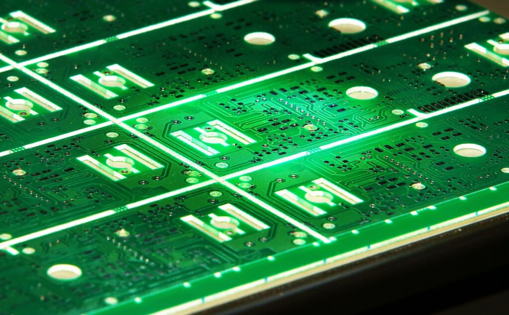
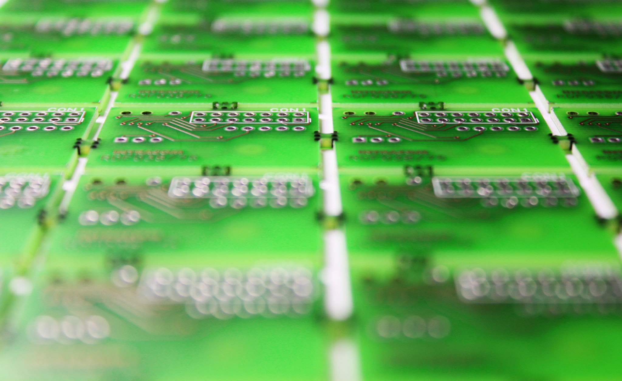
Printed circuit board
To stay at the forefront of the circuit board industry, the team at the 569th EMXS Circuit Board Manufacturing Shop emphasizes continuous training and improvement. Regularly attending conferences, seminars, and training sessions, they strive to enhance their processes and remain up-to-date with the latest advancements in the field. This commitment to ongoing education ensures that they are equipped with the necessary knowledge and skills to deliver high-quality circuit boards that meet the demanding standards of the military.
Manufacturing printed circuit boards for the nation’s military is a responsibility that the team takes great pride in. Hillis acknowledges the weight of their role but finds immense satisfaction in knowing that their work contributes to critical assets for global warfighters. Whether manufacturing new circuit boards or repairing existing ones, the 569th EMXS Circuit Board Manufacturing Shop recognizes the honor and importance of their contribution to the defense and security of the nation.
While the manufacturing process of PCBs may be hidden from the eyes of the end consumer, it is a fascinating journey of precision and expertise. From the initial stages of plating and drilling to the final inspection and testing, each step is a testament to the skill and dedication of the individuals involved. As we continue to rely on increasingly advanced electronics in our daily lives, let us not forget the intricate manufacturing process behind the circuit boards that power our devices and shape the world of technology.
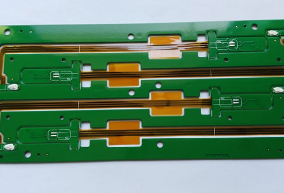
Flexible Printed Circuit Boards (FPCBs) are thin, flexible electronic circuits that are used in a wide range of applications, including smartphones, tablets, wearable devices, and automotive electronics. The manufacturing process for FPCBs involves several steps, including design, material selection, and fabrication.
Design: The first step in FPCB manufacturing is designing the circuit layout. This involves determining the placement of components, the routing of traces, and any necessary connections or vias. Specialized software is used to create the circuit design.
Material Selection: FPCBs are typically made of a flexible substrate material, such as polyimide or polyester film. The choice of material depends on the specific requirements of the application, including flexibility, temperature resistance, and durability.
Copper Cladding: The flexible substrate is coated with a layer of copper on one or both sides. This is typically done through a process called electroless copper plating or electroplating, where a thin layer of copper is deposited onto the substrate surface.
Imaging: A photosensitive material, called a photoresist, is applied to the copper-clad substrate. The circuit pattern is then transferred onto the photoresist using a photomask and exposure to ultraviolet light. This process allows for the creation of the desired copper traces and pads.
Etching: After the imaging process, the exposed copper areas are etched away using an etching solution, leaving behind the desired circuit pattern. The photoresist is then removed, and the substrate undergoes a cleaning process to prepare it for the next step.
Surface Finishing: Surface finishing techniques are employed to protect the exposed copper traces and pads and provide better solderability. Common surface finishes used in FPCB manufacturing include immersion gold, HASL (Hot Air Solder Leveling), and OSP (Organic Solderability Preservatives).
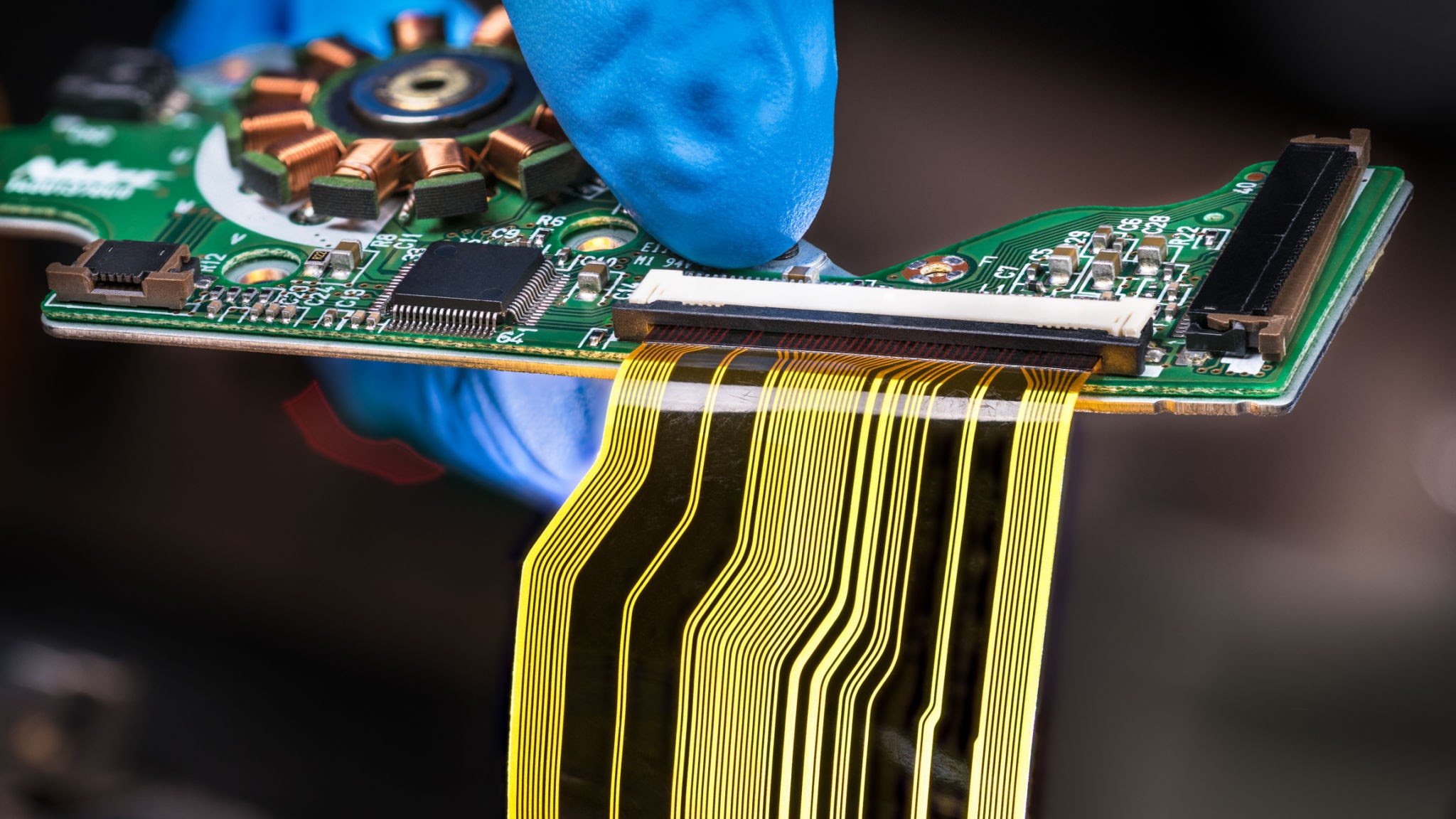
Assembly: Once the FPCBs are fabricated, they can be assembled with electronic components. This involves placing the components onto the FPCB and soldering them in place. The assembly process can be performed using automated equipment or manual labor, depending on the complexity and volume of production.
Equip your facility with the comprehensive PCB manufacturing equipment needed to produce single-sided, double-sided, multilayer, and rigid-flex PCBs efficiently. Streamline your production process with the right tools. Get started today!
Single-Sided FPCB, Double-sided FPCB, Multilayer FPCB, and Rigid-Flex FPCB
To manufacture different types of flexible printed circuit boards (FPCBs), various equipment and processes are involved. Here’s a general overview of the equipment typically used for manufacturing single-sided FPCBs, double-sided FPCBs, multilayer FPCBs, and rigid-flex FPCBs:
Single-Sided FPCB:
Substrate Cutting Machine: Used to cut the flexible substrate (usually polyimide or polyester) into desired shapes and sizes.
Imaging/Exposure Equipment: Used to transfer the circuit pattern onto the substrate through a photosensitive film or dry film resist.
Etching Machine: Used to chemically remove unwanted copper from the substrate, leaving behind the desired circuit pattern.
Plating Equipment: Used for copper electroplating to enhance the copper thickness and ensure good conductivity.
Solder Mask Coating Machine: Used to apply a protective solder mask layer over the copper traces, leaving only the desired areas exposed for soldering.
Surface Finishing Equipment: Used for applying a final finish to the exposed copper surfaces, such as hot air leveling (HASL), immersion gold, or immersion tin.
Double-Sided FPCB:
Same equipment as for single-sided FPCBs, with the addition of the following:
Drilling Machine: Used to drill holes for component leads and vias to establish electrical connections between the two sides of the board.
Electroless Copper Deposition System: Used for depositing a thin layer of copper inside the drilled holes, forming the conductive vias.
Multilayer FPCB:
Same equipment as for double-sided FPCBs, with the addition of the following:
Lamination Press: Used to bond multiple layers of flexible substrates together with adhesive layers.
Bonding Press: Used for bonding inner layers of the FPCB stack with copper foils.
Laser Drilling Machine: Used for high-precision drilling of microvias in the multilayer stack.
Copper Plating Line: Used for through-hole copper plating and subsequent copper buildup on the outer layers.
Additional Imaging/Exposure, Etching, and Plating Equipment: Required for the outer layer circuits.
Rigid-Flex FPCB:
Same equipment as for multilayer FPCBs, with the addition of the following:
CNC Milling Machine: Used for precise cutting and shaping of the rigid sections.
Z-axis Registration System: Ensures accurate alignment between the rigid and flexible sections during lamination.
Additional Drilling and Plating Equipment: Required for the rigid sections.
Please note that specific equipment may vary depending on the manufacturer’s capabilities, technology requirements, and production scale. The above list provides a general idea of the equipment commonly used for manufacturing different types of FPCBs.
What equipment is required to produce single-sided FPCB, double-sided FPCB, Multilayer FPCB, and Rigid-Flex FPCB simultaneously?
If you want to produce single-sided FPCBs, double-sided FPCBs, multilayer FPCBs, and rigid-flex FPCBs simultaneously, you would need a comprehensive set of equipment that can handle the different manufacturing processes involved. Here’s an overview of the equipment you would typically require:
FPCB Manufacturing Machine
If you want to produce single-sided FPCBs, double-sided FPCBs, multilayer FPCBs, and rigid-flex FPCBs simultaneously, you would need a comprehensive set of equipment that can handle the different manufacturing processes involved. Here’s an overview of the equipment you would typically require:
Substrate Cutting Machine: Used for cutting flexible substrates into desired shapes and sizes.
Imaging/Exposure Equipment: Used for transferring circuit patterns onto the substrates using photosensitive films or dry film resists.
PCB Etching Machine: Used for chemically removing unwanted copper from the substrates to form the circuit patterns.
Plating Equipment: Used for copper electroplating to enhance copper thickness and conductivity.
Solder Mask Coating Machine: Used for applying a protective solder mask layer over the copper traces.
Surface Finishing Equipment: Used for applying final finishes to the exposed copper surfaces (e.g., HASL, immersion gold, or immersion tin).
Drilling Machine: Used for drilling holes in the substrates for component leads and vias.
Electroless Copper Deposition System: Used for depositing a thin layer of copper inside the drilled holes to create conductive vias.
Lamination Press: Used for bonding multiple layers of flexible substrates together with adhesive layers in multilayer and rigid-flex FPCBs.
Bonding Press: Used for bonding inner layers of the multilayer and rigid-flex FPCB stack with copper foils.
Laser Drilling Machine: Used for high-precision drilling of microvias in the multilayer stack.
CNC Milling Machine: Used for precise cutting and shaping of the rigid sections in rigid-flex FPCBs.
Z-axis Registration System: Ensures accurate alignment between the rigid and flexible sections during lamination in rigid-flex FPCBs.
Copper Plating Line: Used for through-hole copper plating and subsequent copper buildup on the outer layers in multilayer FPCBs.
Additional Imaging/Exposure, Etching, and Plating Equipment: Required for producing the outer layer circuits in multilayer FPCBs.
Additional Drilling and Plating Equipment: Needed for producing the rigid sections in rigid-flex FPCBs.
It’s important to note that producing all these types of FPCBs simultaneously would require a significant investment in equipment and may involve complex manufacturing processes. It’s advisable to consult with specialized PCB manufacturing equipment suppliers or industry experts to customize a production line that suits your specific requirements and budget.
The U.S. “Protection of Circuit Boards and Substrates Act” is a crucial piece of legislation that aims to safeguard the integrity and security of circuit boards and substrates used in various electronic devices. With the increasing demand for advanced electronic products, many businesses in the United States are considering expanding or building PCB production lines. In this blog, we will provide an interpretation of the Protection of Circuit Boards and Substrates Act, and delve into the essential machinery required in a PCB production line, including PCB etching machines, PCB cleaning machines, PCB drilling machines, PCB browning machines, PCB sandblasting machines, PCB polishing machines, PCB oxidation resistance machines, PCB desoldering machines, PCB stripping machines, and PCB developing exposing machines. This information will help visitors who are motivated to purchase these machines and establish or expand their own PCB production lines.
The “Protection of Circuit Boards and Substrates Act” is a significant legislation aimed at ensuring the security and integrity of circuit boards and substrates used in electronic devices within the United States. The act recognizes the critical role played by circuit boards and substrates in the functioning of electronic products and seeks to prevent unauthorized modifications, counterfeiting, and tampering that could compromise their performance or pose security risks.
The act encompasses various provisions and requirements that manufacturers, distributors, and users of circuit boards and substrates must adhere to in order to comply with the law. Some key aspects of the act include:
Counterfeit Prevention: The act emphasizes the need to combat the production and distribution of counterfeit circuit boards and substrates. It prohibits the manufacturing, sale, or use of counterfeit components and mandates stringent measures to ensure the authenticity of these critical electronic parts.
Traceability and Documentation: The act emphasizes the importance of traceability and documentation throughout the supply chain. Manufacturers and distributors are required to maintain detailed records of the origin, manufacturing process, and distribution of circuit boards and substrates. This information helps establish accountability and facilitates effective quality control and product recalls if necessary.
Quality Assurance: The act promotes the implementation of rigorous quality assurance measures throughout the production process. Manufacturers are encouraged to adopt industry best practices and adhere to recognized standards to ensure the reliability, performance, and safety of circuit boards and substrates.
Security Measures: The act recognizes the need to safeguard electronic devices against potential security threats. It encourages the use of secure designs, authentication mechanisms, and encryption technologies to protect the integrity of circuit boards and substrates. This is particularly relevant in applications where the confidentiality of data or critical operations are at stake.
Compliance and Enforcement: The act establishes mechanisms for compliance verification and enforcement. Regulatory authorities are empowered to conduct inspections, audits, and investigations to ensure that manufacturers and distributors are in compliance with the provisions of the act. Non-compliance can result in penalties, fines, or other legal consequences.
The “Protection of Circuit Boards and Substrates Act” reflects the growing importance of circuit boards and substrates in today’s interconnected and technology-driven world. By establishing guidelines and regulations, the act aims to foster trust among consumers and businesses, protect intellectual property, and promote the safe and reliable use of electronic devices.
For businesses involved in the establishment or expansion of PCB production lines, understanding and adhering to the requirements outlined in the act is essential. Compliance with the act not only ensures legal adherence but also demonstrates a commitment to quality, security, and customer satisfaction.
The Protection of Circuit Boards and Substrates Act focuses on safeguarding the manufacturing, distribution, and use of circuit boards and substrates within the United States. The act imposes regulations to prevent counterfeiting, tampering, and unauthorized modifications to these critical components, ensuring the reliability and security of electronic devices. It is important for businesses engaged in PCB production to adhere to the requirements specified in this act to maintain compliance with the law and protect consumer trust.
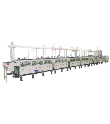
Dragon Etching Customized PCB production line for customers
Dragon Etching Essential Machinery in a PCB Production Line:
PCB Etching Machine: PCB etching machines are vital in the production process as they facilitate the removal of unwanted copper from the substrate, creating the desired circuitry. These machines use chemical processes to dissolve the excess copper, leaving behind the required copper traces for circuit connections.
PCB Cleaning Machine: PCB cleaning machines are used to remove any contaminants or residues that accumulate during the manufacturing process. They employ various cleaning methods such as ultrasonic cleaning, brush cleaning, and chemical cleaning to ensure the cleanliness and reliability of the circuit boards.
PCB Drilling Machine: PCB drilling machines are responsible for creating holes in the circuit boards to accommodate electronic components. These machines utilize high-speed rotating drill bits to accurately drill holes of varying sizes, ensuring precise placement and alignment.
PCB Browning Machine: PCB browning machines, also known as brown oxide machines, are used to create a protective layer on the exposed copper surfaces of the circuit boards. This layer prevents oxidation and enhances the conductivity of the copper traces, improving the overall performance and longevity of the PCB.
PCB Sandblasting Machine: PCB sandblasting machines are employed for surface preparation, primarily to remove solder mask or copper from specific areas. This process is crucial for creating solder pads and ensuring proper solder adhesion during component assembly.
PCB Polishing Machine: PCB polishing machines are used to refine the surface finish of circuit boards. They remove any imperfections, such as rough edges or burrs, resulting from the manufacturing process, and provide a smooth and uniform surface for further processing or component placement.
PCB Oxidation Resistance Machine: PCB oxidation resistance machines apply protective coatings to the circuit boards, safeguarding them against environmental factors such as humidity, moisture, and corrosive substances. These coatings enhance the reliability and durability of the PCBs, ensuring their longevity in demanding applications.
PCB Desoldering Machine: PCB desoldering machines are essential for repairing or reworking PCBs. They allow the removal of electronic components without damaging the board, enabling efficient repairs and replacements during the production process or after device assembly.
PCB Stripping Machine: PCB stripping machines are used to remove unwanted solder masks, ensuring accurate solder pad exposure
PCB etching machines are essential for manufacturing high-quality printed circuit boards (PCBs). Over time, these machines can become contaminated with chemicals and residue from the etching process, which can affect the quality of the etching and potentially damage the machine. To keep your PCB etching machine in top condition, regular cleaning is essential. In this article, we will discuss some tips for using a cleaning solution to clean your PCB etching machine.
Selecting the Right Cleaning Solution: There are several types of cleaning solutions available for cleaning PCB etching machines. It is important to choose a cleaning solution that is safe for the machine and effective at removing the contaminants. Always refer to the manufacturer’s guidelines and recommendations when selecting a cleaning solution.
Protecting Yourself: Before using the cleaning solution, ensure that you are wearing appropriate personal protective equipment (PPE), such as gloves, eye protection, and respiratory protection, if necessary. Cleaning solutions can be corrosive and hazardous, so it is essential to follow proper safety precautions.
Preparing the Solution: Once you have selected a suitable cleaning solution, prepare it according to the manufacturer’s instructions. Typically, the solution will need to be diluted with water to achieve the desired concentration. Use distilled or deionized water, as tap water may contain impurities that can affect the cleaning process.
Cleaning the Machine: To clean the PCB etching machine, apply the cleaning solution to a cloth or sponge and gently wipe down the surfaces. Pay particular attention to areas that are prone to contamination, such as the etching tank, nozzles, and pipes. Avoid using abrasive materials or scrubbers that could damage the machine.
Rinsing and Drying: After cleaning the machine with the solution, rinse the surfaces thoroughly with clean water to remove any remaining residue. Use a clean cloth or paper towel to dry the machine and remove any excess water. It is essential to ensure that the machine is completely dry before using it again, as moisture can cause corrosion and damage to the machine.
In conclusion, cleaning your PCB etching machine with a suitable cleaning solution is essential for maintaining the quality of your PCBs and prolonging the life of your machine. By following these tips, you can help ensure that your machine is clean, safe, and functioning optimally, producing high-quality PCBs that meet your specifications and requirements.
PCBs (Printed Circuit Boards) are essential components of modern electronic devices, providing a platform for connecting and controlling the various components and circuits that make up the device. PCBs are typically manufactured using a chemical process that involves etching the copper traces and pads on the board using a chemical solution. While this process is generally safe and effective, there are some cautions that should be taken when handling and working with the chemicals involved.
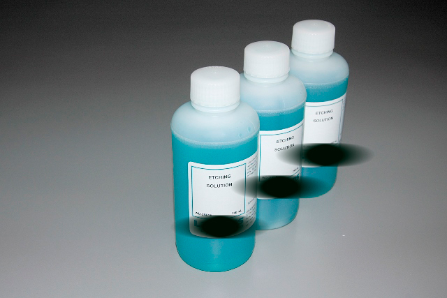
Choose the right etching solution: There are several different types of etching solutions available, each with its own properties and advantages. Some of the most commonly used etching solutions include ferric chloride, ammonium persulfate, and sodium persulfate. Before selecting an etching solution, consider the type of PCB you are manufacturing, the desired trace widths and depths, and the cost and availability of the solution.
Ventilation: ThePCB etching process can produce harmful fumes and vapors, which can be toxic if inhaled in large quantities. It is essential to work in a well-ventilated area, preferably with an exhaust hood or other ventilation system, to prevent the buildup of fumes and vapors.
Cleanliness: PCBs must be thoroughly cleaned after the etching process to remove any residual chemicals and prevent contamination. Use a suitable cleaning solution and ensure that all equipment, tools, and surfaces are cleaned regularly to maintain a safe and clean working environment.
Dilution: Etching solutions are typically used in a diluted form, as the concentrated solution can be too aggressive and damage the board. It is essential to dilute the solution correctly, following the manufacturer’s instructions and using the correct ratio of solution to water. Be sure to use distilled or deionized water, as tap water may contain impurities that can affect the etching process.
Temperature: The temperature of the etching solution can have a significant impact on the etching process, affecting the speed and quality of the etch. Most etching solutions work best at a specific temperature range, typically between 35°C and 50°C. Use a thermometer to monitor the temperature of the solution and adjust as needed to maintain the desired temperature.
Agitation: Agitation of the etching solution is important for ensuring an even and consistent etch. This can be achieved by using an agitation system, such as a pump or bubbler, or by manually agitating the solution using a stirring rod. Ensure that the agitation is not too strong, as this can damage the board, or too weak, as this can result in uneven etching.
Safety measures: It is essential to follow proper safety procedures when working with PCB etching chemicals. Store the chemicals in a secure location away from children and pets, and dispose of them properly in accordance with local regulations. Avoid mixing different chemicals or using them in unintended ways, as this can cause dangerous reactions.
Safety: Etching solutions are corrosive and can cause skin and eye irritation, respiratory problems, and other health issues if not handled properly. Always wear protective gear, such as gloves, goggles, and a respirator, when handling etching solutions. Store the solutions in a secure location away from children and pets, and dispose of them properly in accordance with local regulations.
By following these etching solution usage tips, you can help ensure a successful and safe etching process, resulting in high-quality PCBs that meet the required specifications and performance standards.
Learn about the benefits of using rigid flex PCBs, including their production process and use cases such as fingerprint technology. Discover top manufacturers and the equipment required for production.
igid-flex PCBs, also known as hybrid PCBs, are a combination of rigid and flexible circuit boards that are interconnected by plated through-holes. These circuit boards offer a variety of advantages over traditional PCBs, including increased reliability, reduced weight and space requirements, and enhanced design flexibility. In this article, we’ll explore the advantages of rigid-flex PCBs, their production process, and some of their common applications.
What is Rigid Flex PCB?
Rigid-flex PCBs are a type of printed circuit board that combines the characteristics of rigid and flexible circuits into a single design. These boards consist of multiple layers of flexible circuitry, which are laminated together with layers of rigid circuitry. The flexible sections of the board are typically used to connect components, while the rigid sections are used to mount components and provide mechanical stability.
Advantages of Rigid-Flex PCBs:
Increased Reliability: The flexibility of these circuit boards makes them less susceptible to damage from mechanical stresses, vibration, and thermal expansion, which can improve their reliability.
Reduced Weight and Space Requirements: The use of flexible circuitry can reduce the overall weight and size of the board, making them ideal for use in portable devices and other applications where space is limited.
Enhanced Design Flexibility: The use of flexible circuitry also allows for more complex and intricate designs, which can improve performance and reduce manufacturing costs.
Improved Signal Integrity: The use of flexible circuitry can reduce the number of interconnects required, which can improve signal integrity and reduce the potential for interference.
Cost-Effective: Despite their many advantages, rigid-flex PCBs can be produced at a cost that is comparable to traditional PCBs, making them an attractive option for a wide range of applications.
Production Process of Rigid-Flex and Flexible PCBs:
The production process of rigid-flex PCBs involves several steps, including design, fabrication, and assembly. The design process typically involves the use of computer-aided design (CAD) software to create a 3D model of the board. This model is then used to generate the necessary manufacturing files, which are used to produce the board.
The fabrication process for rigid-flex PCBs involves a combination of flexible and rigid circuit board manufacturing techniques. The flexible circuitry is typically produced using a photo-etching process, while the rigid circuitry is produced using a subtractive or additive process.
Once the circuit boards have been produced, they are assembled together using plated through-holes, which are used to create electrical connections between the different layers of the board. The assembly process also involves the placement of components, which are then soldered onto the board.
Use of Fingerprint Rigid-Flex PCB:
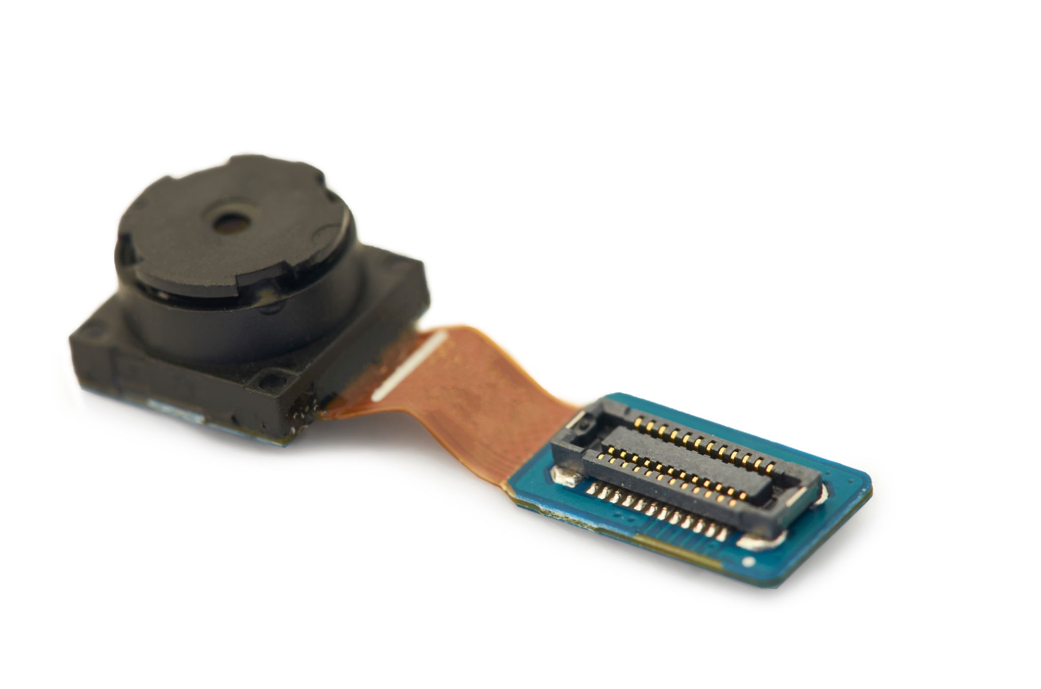
One of the most common applications of rigid-flex PCBs is in fingerprint sensors. These sensors require a high degree of flexibility, which can be achieved using flexible circuitry. The rigid sections of the board are used to mount the sensor components and provide mechanical stability.
Cost:
The cost of producing rigid-flex PCBs can vary depending on the complexity of the design, the number of layers, and the volume of the order. However, rigid-flex PCBs are typically more expensive than traditional PCBs due to the additional manufacturing steps and materials required.
Famous Manufacturers:
Some of the well-known manufacturers of rigid-flex PCBs include:
The production of rigid-flex PCBs requires several specialized pieces of equipment, including:
Etching machine: This machine is used to remove unwanted copper from the surface of the PCB using a chemical solution. It typically consists of a tank filled with the etchant solution, and a mechanism for moving the PCB through the solution.
Plating machine: This machine is used to add a layer of metal to the surface of the PCB in order to enhance its electrical conductivity and protect it from corrosion. It typically consists of an electroplating bath containing a solution of metal ions, and a mechanism for applying an electric current to the PCB.
Photoresist equipment: This equipment is used to apply the photoresist material to the surface of the PCB, and to expose it to UV light in order to selectively harden the photoresist in the areas where the copper is to be retained.
Clean room facilities: Clean rooms are used to prevent contamination of the PCB during production, and to ensure that the final product meets the required quality standards. Clean rooms typically have controlled air flow, humidity, and temperature, and are equipped with specialized equipment for handling and assembling PCBs.
Testing and inspection equipment: Once the PCB has been produced, it must be tested and inspected to ensure that it meets the required quality standards. This typically involves using specialized equipment to test the electrical conductivity and other properties of the PCB, and to inspect it for defects and other issues.
This website uses cookies so that we can provide you with the best user experience possible. Cookie information is stored in your browser and performs functions such as recognising you when you return to our website and helping our team to understand which sections of the website you find most interesting and useful.
Strictly Necessary Cookies
Strictly Necessary Cookie should be enabled at all times so that we can save your preferences for cookie settings.
If you disable this cookie, we will not be able to save your preferences. This means that every time you visit this website you will need to enable or disable cookies again.