Advanced FeCl₃ Regeneration Methods
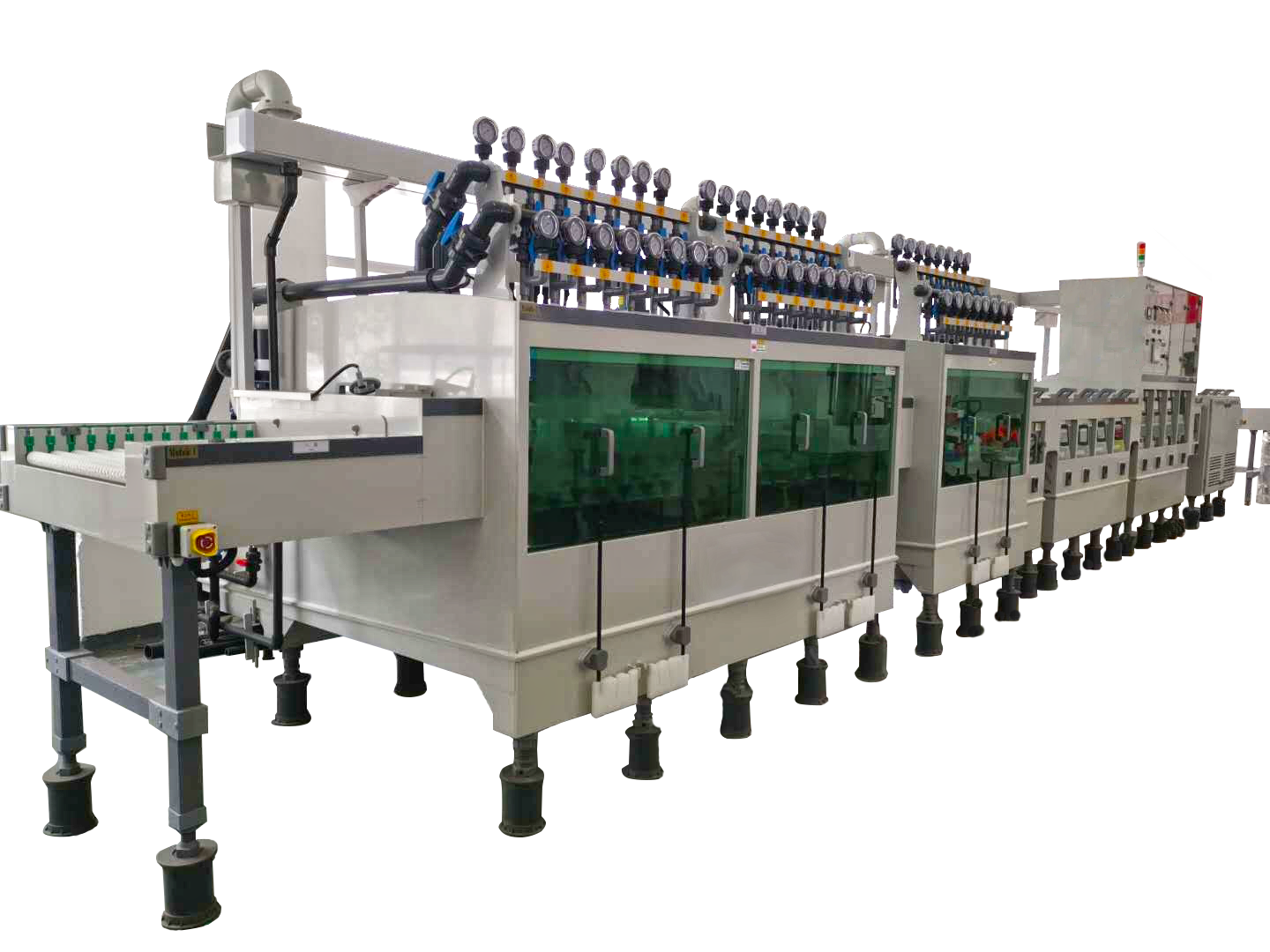
Copper etching for PCB manufacturing can produce significant chemical waste, which presents environmental and economic challenges. To minimize waste and improve efficiency, advanced methods for regenerating Ferric Chloride (FeCl₃) are increasingly being implemented. Two notable techniques include:
pH Adjustment
pH adjustment is a simple yet effective way to regenerate FeCl₃. By adjusting the pH to an optimal range (typically between 1.5 and 2.0), the solution can maintain its etching capability for longer periods, reducing the need for fresh etchant. This method helps reduce both chemical waste and operating costs.
Electrolytic Recovery
Electrolytic recovery uses electrical current to reduce ferric ions (Fe³⁺) back to ferrous ions (Fe²⁺), effectively restoring the etching solution’s strength. This method not only recycles the etchant but also ensures that its activity remains consistent, which is crucial for high-precision PCB etching. Electrolytic recovery systems can be integrated into the etching process to continuously regenerate the solution, minimizing waste.
Undercut Control Strategies
One of the key challenges in copper etching is controlling undercutting – the lateral removal of material beneath the maskant, leading to undesirable etching results. Below are some strategies for improving adhesion and reducing undercutting:

Maskant Adhesion Tests
The type of maskant used in the etching process plays a crucial role in minimizing undercut. Two common types of maskants are dry film and liquid photoresist. Both have distinct performance characteristics:
| Maskant Type | Advantages | Disadvantages |
|---|---|---|
| Dry Film | Higher precision, easier to apply on complex geometries | More expensive, prone to contamination during application |
| Liquid Photoresist | Cost-effective, simpler to apply | Lower precision, more prone to undercutting if not applied correctly |
Testing the adhesion of both maskants under different conditions helps determine which type is best suited for reducing undercut in specific applications.
Data-Driven Analysis

Utilizing data-driven analysis can greatly improve the accuracy and consistency of the etching process. For instance, the etch rate of copper can vary depending on temperature and etchant concentration. The following graph shows the relationship between the etch rate (μm/min) and temperature (ranging from 20°C to 50°C) for a 35% FeCl₃ solution:
Graph: Etch Rate vs. Temperature for 35% FeCl₃
| Temperature (°C) | Etch Rate (μm/min) |
|---|---|
| 20 | 5.2 |
| 25 | 6.1 |
| 30 | 7.8 |
| 35 | 9.3 |
| 40 | 11.2 |
| 45 | 13.0 |
| 50 | 14.5 |
This data shows that as temperature increases, the etch rate increases, which is a typical behavior for most etching solutions. However, process engineers should balance temperature control to avoid issues like excessive etching or damage to the PCB.
Case Study: Reducing Side-Etching by 40% in 6-Layer PCB Production Using Pulsed Spray Etching
In a recent case study, a 6-layer PCB manufacturer faced challenges with side-etching, where copper was etched unintentionally along the edges of traces, compromising the overall performance of the circuit. By switching to pulsed spray etching, the manufacturer achieved a 40% reduction in side-etching.
Key Findings:
- Pulsed spray etching delivers etchant in short, controlled bursts, which helps to improve material removal consistency and reduce the time the PCB is exposed to the etching solution.
- The improved uniformity in etch distribution resulted in less lateral copper loss during the etching process, thus improving the final product quality.
This case study demonstrates how innovative etching techniques can lead to better results in high-density PCB manufacturing.
Pro Tip: Maintain Etchant Density at 1.32–1.38 g/cm³ for Consistent Results (Baumé Scale)
Maintaining the proper etchant density is crucial for achieving consistent results in copper etching. For FeCl₃, density should be maintained between 1.32–1.38 g/cm³ (measured on the Baumé scale) to ensure optimal etching performance. Variations in density can lead to changes in the etch rate, which can affect etching precision and PCB quality. Regular monitoring and adjustments of etchant density are essential to maintain consistency throughout the production process.
In conclusion, optimizing copper etching for PCB manufacturing involves adopting advanced methods such as FeCl₃ regeneration, controlling undercutting, and leveraging data-driven analysis. With careful management of process variables and the integration of innovative techniques like pulsed spray etching, process engineers can significantly improve both efficiency and quality in PCB production.
For more information on etching technologies and case studies, check out this insight from PCBTech on innovative etching techniques used in the industry.